Are you sure reverse recovery is going to factor into your dissipation calcs? Won't there be a fast rectifier, maybe even a SiC Schottky or some such doing that conducting?
So easy to get seduced by a 650V, 11A, USD $6,45 device that is that fast, but getting that miniscule 1,4W out of a part that is bottom-surface-cooled and only 5 by 6 millimeters is still gonna be a challenge.😉 Driving one properly isn't much fun, either.
A lot of those fine dual-MOSFET driver ICs are disqualified by too-low of a UVLO spec. Still others have to be put through contortions to provide the recommended small negative turn-off bias.
If its still just too tempting, you might have a look at the offerings from Transphorm -- a depletion-mode GaN, cascode-connected to a regular N-ch MOSFET, in a standard package, and they accept 'standard' drive signals.
Prices are decent, too. Just a thought ..
Cheers
I could add a diode instead of using the body diode but that's an expensive inferior solution. I have used GaN before up to 27 MHz I should be fine 😉 (resonant converter, quasi resonant gate drive). Negative gate drive isn't a desired thing with GaN as it increases the losses during the reverse conduction during dead-time, sometimes its recommended to stop inadvertent turn on due to the effective Cgd but if the drive pull down is low enough impedance and the package has low enough inductance it should not be required.
My go to gate drive used to be the Peregrine semi low side driver (sub nS switching) and then if I needed a floating drive using RF baluns as signal transformers to level shift and a load of floating supplies. However this part is discontinued and there is no need for such speed here. So I was thinking Si8274GB1-IM1 (3V UVLO) with a regulated 6V bootstrap for the high side.
I only didn't go straight to GaN because I wanted to be able to assemble the boards myself for prototyping in case I blew a device. I have soldered the GaN systems packages before but I don't have a board pre-heater at home which is required. (also GaN has had a price drop it used to be pricey)
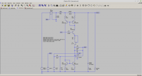
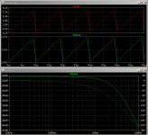
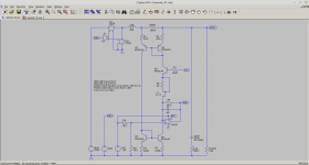
I think the simulation is valid as this is a current sensor so I'm measuring its transfer function.
OK, sorry, understand what you are saying. Poking about it seems to be a problem local to the opamp that might be exacerbated by my bucket of transistors. I'll go back and fiddle some more. The bucket of transistors may have been a bad idea. No doubt you will have realised that I really do not know exactly what I am doing. It does however still look tameable on a single supply.
In respect of losses one thought that crops up which might not alleviate such concerns is the use of a synchronous buck stage. You can place your bulk storage on the PFC but operate with a reduced capacitance at the buck output because it can source and sink current, regenerate or boost back to the input. That would need bidirectional current sensing at which point +/- supplies could be beneficial.
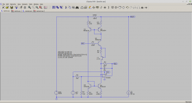
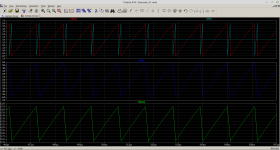
Redone for bi-directional operation. Still single supply. Nominally 2.5V out for zero Amps and 100mV per amp. Some gain and offset errors.
...
...
Attachments
Last edited:
Fancy current sense!
I have built bi-directional power converters before, to be avoided very difficult.
I played around with the GaN Systems double pulse simulation and am pretty satisfied that the Si gate drive will work and losses will be under control. Back of envelope calculations indicate I will be able to get the heat out of the devices via thermal vias. I find beyond very basic calculations on these kind of things you have to do experiments though as the alternative is EM simulation and thermal simulation which in the circumstance that I'm pretty sure its going to work takes longer.
Attachments
Yeah . . 😱 how easily I forget there are darned-sharp designers on here -- some even with piles more experience than me ..
Guess I'm still kinda stuck in the mind-rut from a while back -- couldn't seem to talk a guy out of the idea to just pop some GaN FET's into a regular MOSFET design 'and get much better sound quality!' Sorry.
Thanks for the negative Gate drive tip, too.
Cheers
Guess I'm still kinda stuck in the mind-rut from a while back -- couldn't seem to talk a guy out of the idea to just pop some GaN FET's into a regular MOSFET design 'and get much better sound quality!' Sorry.
Thanks for the negative Gate drive tip, too.
Cheers
the philips stewardess travel iron is an ideal hotplate at low cost.
I have one with the thermstat altered such that it can provide temperatures till 200degrC.
Dry iron HD1301/02 | Philips
I have one with the thermstat altered such that it can provide temperatures till 200degrC.
Dry iron HD1301/02 | Philips
Fancy current sense!
I have built bi-directional power converters before, to be avoided very difficult.
I suppose the fun arises because the loudspeaker is a motor and recovering power/energy back from it into the PFC capacitance might prove to be interesting.
It might be premature so I'll fall flat on my face but a simple buck with a catch diode operates with discontinuous inductor current up to a load of half the inductor ripple. Synchronous buck operates with continuous inductor current at all times. It should be possible to operate with ZVT up to a load of half the ripple current. It should also be the case that switch turn off occurs after currents have reversed in the on switch such that the body source diode is no longer conducting so you do not suffer from Trr losses.
The penalty being that extending that range incurs higher RMS on losses due to the higher inductor ripple current.
Naive analysis follows. Recreates Dixons average current mode control gain derivation.
For the buck convertor during Ton the inductor is set through (VIN-VOUT). During Toff the inductor is reset through VOUT. Steady state the average inductor current remains the same.
dIon = (VIN-VOUT)Ton/L
dIoff = VOUT.Toff/L
(VIN-VOUT)Ton = VOUT.Toff
Call Ton the operating duty cycle D. Toff becomes (1-D)
(VIN-VOUT)D = VOUT(1-D)
Things get normalised to 1 second.
Multiply out and rearrange to get
D = VOUT/VIN
Peturb the operating duty cycle by a small amount p
D -> (D + p)
(1-D) -> (1-D-p)
The change in setting volts become
dVon = (VIN-VOUT)(D+p)
The change in resetting volts become
dVoff = VOUT(1-D-p)
The change in voltage applied across the inductor becomes
dVL = (VIN-VOUT)(D+p) - VOUT(1-D-p)
Multiply out and substitute for D
dVL = pVIN
With VIN regulated which it kind of will be as a result of the PFC preregulator this is fixed. We also have VFF in the UCC35705 to polish things off.
This results in a change in current through the inductor of
dIL = pVIN/2PIfL
converted to a change in current across the current sense resistor, -j omitted.
dVrsns = pVINRsns/2PIfL
The original perturbation arises from a change in the Current Error Amplifier output compared to the PWM modulator ramp Vs
p = dVcea/Vs
dVrsns = dVceaVINRsns/2VsPIfL
dVrsns/dVcea = VINRsns/2VsPIfL
This is the control to output response or our Power Circuit Gain, Gpow. -j magically appears.
Gpow = -jVINRsns/2VsPIfL
As per slope matching the slope at the output of the CEA must not exceed the slope of the ramp. This sets the maximum gain in the CEA at the switching frequency. Depending on the sense of the modulator, leading or trailing edge, this can be during switch on time or switch off time. Other considerations may arise as a result.
In out case the UCC35705 is acting as a leading edge modulator and the slope to be matched occurs during switch off time. As such the rate of the slope depends on VOUT which means we have to calculate based on maximum VOUT.
During the switch off time
dIL/dT = VOUT/L
converted in the sense resistor to
dVrsns/dT = RsnsVOUT/L
Amplified by the CEA
dVcea/dT = GceaRsnsVOUT/L
For slope matching
dVcea/dT = dVs/dT
With a switching frequency of Fs and ramp amplitude Vs
dVcea/dT = Fs.Vs
GceaRsnsVOUT/L = Fs.Vs
Giving the maximum gain in the CEA as
Gcea = Fs.Vs.L/RsnsVOUT
Loop gain is power circuit gain multiplied by error amplifier gain
Gl = GceaGpow
Gl = Fs.Vs.L/RsnsVOUT X -jVINRsns/2VsPIfL
Gl = -jVIN.Fs/2VOUTPIf
Substitute for VIN/VOUT = 1/D and
Gl = -jFs/2PIDf
Set to unity and the crossover frequency becomes
Fco = Fs/2PID
Last edited:
Conceptually... With VIN=400V, VOUT=360V, Fs=100KHz and a nominal 5A load you would design for a ripple current in the inductor of 10A which would be 36uH and knock it down/up a bit so use 30uH
The result is reversal of current in the on switch prior to turn off so the body diode is taken out of the equation and, with inserted dead time, the remaining inductor current positions the opposite switch for ZVT.
Of course that falls over if you transition the 5A boundary so you could design for more ripple but as with all of this stuff it's down to choices.
...
Attachments
Last edited:
If a loudspeaker works anything like a BLDC motor no special effort is required to recover the reactive energy input to the DC bus. In fact I think this is described as 'bus pumping' for half bridge amplifiers.
As for moving the capacitance to the PFC stage I think this is what Powersoft are doing as it gives a big advantage that with only a small amount of capacitance on the buck stage you can then adjust the amplifier rail voltage. Their amps run with a short digital delay to allow envelope modulation of the power rails:
R&D Stories: Future Shock. Powersoft Audio’s Amplifier Technologies | audioXpress
The powerflow should be net towards the speaker though so I don't see any advantage of making the buck stage bidirectional.
Diyaudio should have Latex maths input...
Diyaudio should have Latex maths input...
Heard of it but don't use it. Perhaps I should have used the # tag.
LaTeX and users thereoff should STFU and stop messing with my Google searches.
> If a loudspeaker works anything like a BLDC motor no special effort is required to recover the reactive energy input to the DC bus.
Many spinning motors carry enough copper to give efficiency >90%.
Efficiency of a vibrating speaker with too-light winding is rarely >5%.
The round-trip losses are 20% for motor and 99% for the speaker. The 80% is worth recovering, the 1% isn't.
If the bass player sits on the speaker resonance you may get half your energy coming back, and need to allow for that... except this is half of the small energy absorbed in a high impedance (>50r).
Some interesting numbers on the GaN systems bottom side cooled parts. The thermal pad is 4.41 x 2.23 mm which allows for 18, 0.3mm diameter thermal vias without exceeding the pad size. If the board is made from 1 mm thick material and uses 2oZ copper (Including plating the vias the 2oZ which may be expensive) the thermal resistance of these vias is 2.75c/W. This looks great as GaN systems own app notes on these devices typically have a much larger via area than the pad to get the heat out.
Where things start to fall apart a bit thermally is getting the heat off a small area of PCB, ideally you would use one large thermal pad for the whole bottom of the PCB. So you would be looking at something like a 1.2W/mk pad of 0.5 mm thickness. Assuming the bottom layer is expanded to be the whole 5 x 6 mm of the device and not including spreading resistance the thermal resistance of the pad would be 13.9c/W. That's too high so a greater area than the device will be required to get the heat out of the device.
I have seen a number of solutions that could result in greater power density:
1. Hard anodized heat sinks (electrical insulation) and indium metal or thermal paste. Very high performance and expense.
2. Machined base plate such that the majority of the board can be insulated electrically with air and high performance thermal interface material is used in the small contacted areas under the devices.
Hi andrewlebon, whats the taget power output?
I found a big problem with directly screwing down the board onto the heatsink is that I need to use snap in capacitors to get sufficient capacitance which have leads poking down. So I have a 3rd solution that should be easy for me to fabricate for the prototypes and is adaptable into solution 2 for a production version (if I ever get so far).
3) use a 0.5mm thick piece of aluminum with some holes drilled in it underneath the devices. Stackup:
Device, PCB top layer, Thermal vias, PCB bottom layer, electrical insulator, 0.5 mm aluminum, thermal paste, heatsink.
The legs of the caps will be quite close to the heatsink so I will put an insulation sheet between the heatsink and the board but this no longer has to be an expensive thermal interface material.
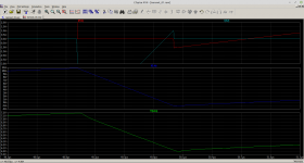
Simulated energy storage system performance
I have simulated how the energy storage will respond with typical program material. Looks good peak power into 8ohms is ~10 kW and the supply fully recovers in time for the next beat with 10mF of capacitance. Find attached simulations and my notes.
I have simulated how the energy storage will respond with typical program material. Looks good peak power into 8ohms is ~10 kW and the supply fully recovers in time for the next beat with 10mF of capacitance. Find attached simulations and my notes.
Attachments
A bit more thermal work on the GS0650111L, approximate numbers indicate needing to keep <6.8W per device dissipation. I had to up the number of thermal vias as I checked the plating depth that allPCB achieves for their vias and its much less than what is achieved on the top/bottom layers. High end solutions to getting more heat out would be copper coin inserts or filled vias or using aluminum core PCB inserts, however a key objective of this design is to be cheap! so non standard PCB work is out.
I'm going to try using:
SimScale - CFD, FEA, and Thermal Simulation in the Cloud | CAE
to simulate my thermal conductivity
There is some good info on via performance here:
https://gansystems.com/wp-content/u...rmal-Design-Guide-Enhancement-Mode-031815.pdf
I'm going to try using:
SimScale - CFD, FEA, and Thermal Simulation in the Cloud | CAE
to simulate my thermal conductivity
There is some good info on via performance here:
https://gansystems.com/wp-content/u...rmal-Design-Guide-Enhancement-Mode-031815.pdf
Attachments
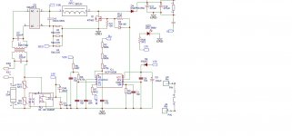
In terms of the power supply my current plan is to use an interleaved PFC...
Did you ever finish this?
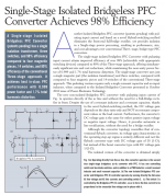
You may be interested in Cuk's latest PFC, seems to solve all your issues, isolated too if you want.
PETarticles.pdf - Google Drive
Best wishes
David
Attachments
Last edited:
- Home
- Amplifiers
- Power Supplies
- Energy storage in non isolated amplifier PFC stage