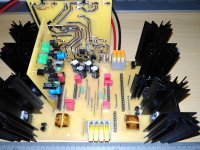
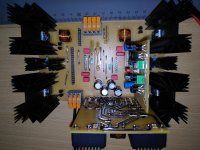
Alright, good news! I finished up all the boards required to get one channel up, and also just tested the auto-bias functionality, which works perfectly fine! The quiescent current of the output pair is 100x the current generated by U2 on the OTA schematic (minus some small bias currents here and there), just as intended, and completely independent of temperature.
I'll add the LTP board next and then test the amp's overall stability.
The OTA board is way too complicated, though... I'll definitely have to simplify it once everything works.
The second channel is already populated on the amp's main board, except for its fuses, so half of the board is currently disabled until I've tested the first channel - then I'll make another pair of OTA and LTP boards for the second one.
Attachments
Last edited:

It's a very interesting circuit.
In #10 schematic, I think that Q14 and Q15 can also be deleted by deleting Q10 and Q11 and adjusting it so that the reference current (1.5mA) flows from Q9 to Q12 through "multiplication square root circuit" at quiescence, did you also think?
Silly question, what does OTA stand for?
I look forward to seeing the progress.
Last edited:
I've played with that idea, but decided that it'd be better for the prototype to have independent control of the 1.5mA reference current so that the two stages - auto-bias and voltage feedback - influence each other as little as possible. If I recall correctly, I had a bandwidth problem in the voltage feedback stage that necessitated more bias current through it; in the posted circuit, it runs at 5mA. You're right that this is one point where a 2nd version of the circuit could save a lot of parts, at the expense of coupling the reference current of the auto-bias stage to the quiescent current of the voltage feedback stage. That shouldn't really be a problem though as I plan on removing the quiescent current potentiometer in the second version anyway.In #10 schematic, I think that Q14 and Q15 can also be deleted by deleting Q10 and Q11 and adjusting it so that the reference current (1.5mA) flows from Q9 to Q12 at quiescence, did you Also think?
"Operational Transconductance Amplifier" - an OpAmp with a current output instead of a voltage output. The voltage feedback stage is implemented as an OTA with two identical outputs, which is why I'm calling that board the "OTA board". The LM13700 is an example of an integrated OTA (a very interesting part for audio applications).Silly question, what does OTA stand for?
Thanks, I'll keep you updated! 👍I look forward to seeing the progress.
Seeing here and IanHegglun's thread, I also pulled out the non-switching output prototype in the barrack state that I built two years ago from a corner of the storeroom.


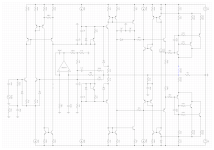
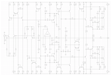
Q1, Q2, Q9, and Q10 form a multiplication square root circuit. For heat dissipation and temperature tracking, these transistors are attached to another aluminum L-angle machined heatsink.

The ratio of the output stage bias current and the reference current flowing from Q1 to Q2 is determined by the ratio of the saturation currents “Is” of the C5198/A1941 and TTC004/TTA004. Since it is difficult to determine the bias current by calculation, it is possible to adjust the value of R2.
Diode-connected Q9 and Q10 deviate from the exponential function characteristics due to parasitic resistance and other factors when a large current flows.
Therefore, Icn * Icp = constant does not hold true, but it is OK as long as there is no cutoff.
Your method of having a diode in parallel with the sense resistor to hold enough current even in the off-side transistor might be a good approach.
My drive circuit (OTA?) uses the power supply current of the operational amplifier used in Alexander amplifiers etc. as an output.
The power supply voltage is limited to ±20V or less because the board of the small output amplifier that I made earlier is used and the cascode of the op amp is omitted. We plan to eventually add a cascode to allow for a larger swing.
The OPA828 I am using is very excellent and I think it is suitable for this circuit.
Q1, Q2, Q9, and Q10 form a multiplication square root circuit. For heat dissipation and temperature tracking, these transistors are attached to another aluminum L-angle machined heatsink.
The ratio of the output stage bias current and the reference current flowing from Q1 to Q2 is determined by the ratio of the saturation currents “Is” of the C5198/A1941 and TTC004/TTA004. Since it is difficult to determine the bias current by calculation, it is possible to adjust the value of R2.
Diode-connected Q9 and Q10 deviate from the exponential function characteristics due to parasitic resistance and other factors when a large current flows.
Therefore, Icn * Icp = constant does not hold true, but it is OK as long as there is no cutoff.
Your method of having a diode in parallel with the sense resistor to hold enough current even in the off-side transistor might be a good approach.
My drive circuit (OTA?) uses the power supply current of the operational amplifier used in Alexander amplifiers etc. as an output.
The power supply voltage is limited to ±20V or less because the board of the small output amplifier that I made earlier is used and the cascode of the op amp is omitted. We plan to eventually add a cascode to allow for a larger swing.
The OPA828 I am using is very excellent and I think it is suitable for this circuit.
Alright, I've got some preliminary results! Unfortunately, the Mornsun DC/DC bricks I used to turn 12V into isolated +/-15V turned out to be an absolute EMI disaster (who could've seen that coming), so the THD measurements are full of radio-frequency interference, which makes the spectrum look terrible.
Output spectrum @ 1kHz, driving approximately 12W into 5 Ohms (8Vrms), which is full power for this small test version of the amp:

And 10kHz, same amplitude:

In numbers, THD+N at full power into 5 Ohms and with tons of radio frequency interference from the DC/DC converters is:
I've also built a little CS4816 + ES9023 Toslink receiver board that plugs into the amp to drive it directly with an optical signal. I'll post schematics and layouts of that thing later, too, once I've sorted everything out.
Output spectrum @ 1kHz, driving approximately 12W into 5 Ohms (8Vrms), which is full power for this small test version of the amp:
And 10kHz, same amplitude:
In numbers, THD+N at full power into 5 Ohms and with tons of radio frequency interference from the DC/DC converters is:
- -78dB at 1kHz (0.013%)
- -70dB at 10kHz (0.032%)
I've also built a little CS4816 + ES9023 Toslink receiver board that plugs into the amp to drive it directly with an optical signal. I'll post schematics and layouts of that thing later, too, once I've sorted everything out.
Do DC-DC converters have common mode chokes?
In the past, when I used an isolated DC-DC converter in a power amplifier circuit where a bootstrap floating power supply was required, switching noise appeared.
Inserting a common mode choke on the primary side of the DC-DC converter improved it considerably.
A choke with a large inductance is effective because the switching frequency is low.
Do DC-DC converters have common mode chokes?
In the past, when I used an isolated DC-DC converter in a power amplifier circuit where a bootstrap floating power supply was required, switching noise appeared.
Inserting a common mode choke on the primary side of the DC-DC converter improved it considerably.
A choke with a large inductance is effective because the switching frequency is low.
These particular converters are sadly a bit more problematic than that... The small unregulated DC/DC bricks you'd normally use for bias voltages are forward converters, which means that they don't produce too much interference on the secondary side - there's just an oscillator, transformer, and rectifier in them. The ones I used in my design are large 60W bricks (120W total across the positive and negative rails), which are constructed quite a bit differently. They use a flyback topology internally, as well as synchronous rectification, which makes them incredibly noisy on the secondary side. They also switch at very high frequencies close to 500kHz. Adding a common-mode choke unfortunately won't easily fix this since the noise is differential-mode (excessive high frequency ripple). I can't add more capacitance to the output either as that'd make the converters unstable.
I'll just use a normal mains transformer for testing and build a lower noise DC/DC module later.
The converters are Mornsun URB2415LD-60WHR3.
HiFi devices are best kept away from switching power supplies.Alright, I've got some preliminary results! Unfortunately, the Mornsun DC/DC bricks I used to turn 12V into isolated +/-15V turned out to be an absolute EMI disaster (who could've seen that coming), so the THD measurements are full of radio-frequency interference, which makes the spectrum look terrible.
Output spectrum @ 1kHz, driving approximately 12W into 5 Ohms (8Vrms), which is full power for this small test version of the amp:
Took a little longer than expected again, but I've finally built myself a low ripple transformer PSU and redid the THD+N measurements with that (instead of the noisy switcher).
The results look very promising! The amp manages to do -80dB THD+N at 1kHz and full power output (8 Vrms into 5 Ohms), and -75dB at 10kHz, same amplitude and load. Noise floor is basically nonexistent (about -120dB), which is quite surprising given the sheer complexity of this amp's circuitry (with its three nested feedback loops).
THD spectra (1kHz, 10kHz, measured at the load resistor using a Steinberg UR12 audio interface):


Measurement setup:

The amp takes Toslink directly to eliminate any kind of grounding / interference issues when connected to my computer. I just used Audacity to play a sinewave via that Toslink connection. The Toslink daughterboard uses a CS8416 SPDIF decoder and ES9023 DAC. The UR12 is connected to a high-power resistive divider, which doubles as the load.
Also, @IanHegglun was spot-on with his prediction that the THD won't change much at higher frequencies! Seems like the auto-bias loop is doing its job properly and operates fine at audio frequencies even in the real world.
I might do another measurement with a better audio interface (MOTU M4) once I've got that set up properly with GNU Radio. I'm not sure if that'll change much, though.
Next up will be a better power supply (resonant SMPS, with sinusoidal waveforms for low EMI), as well as a little speaker protector board.
The results look very promising! The amp manages to do -80dB THD+N at 1kHz and full power output (8 Vrms into 5 Ohms), and -75dB at 10kHz, same amplitude and load. Noise floor is basically nonexistent (about -120dB), which is quite surprising given the sheer complexity of this amp's circuitry (with its three nested feedback loops).
THD spectra (1kHz, 10kHz, measured at the load resistor using a Steinberg UR12 audio interface):
Measurement setup:
The amp takes Toslink directly to eliminate any kind of grounding / interference issues when connected to my computer. I just used Audacity to play a sinewave via that Toslink connection. The Toslink daughterboard uses a CS8416 SPDIF decoder and ES9023 DAC. The UR12 is connected to a high-power resistive divider, which doubles as the load.
Also, @IanHegglun was spot-on with his prediction that the THD won't change much at higher frequencies! Seems like the auto-bias loop is doing its job properly and operates fine at audio frequencies even in the real world.
I might do another measurement with a better audio interface (MOTU M4) once I've got that set up properly with GNU Radio. I'm not sure if that'll change much, though.
Next up will be a better power supply (resonant SMPS, with sinusoidal waveforms for low EMI), as well as a little speaker protector board.
@ttlhacker -- the Linear Tech (now Analog Devices) low noise gate drivers might fit the bill for low noise. Most of the new ones are pretty small, but the LT1683, an older SOIC device, is still in production.
Hello all! First of all, I want to congratulate you on the design. I've been over several variations of simulating it, and I gotta say it acts flawlessly. There's just a few things I would tweak/add to further improve it. For instance CFB amps are notoriously known for not-so-great DC offset on the output. I would definitely add a servo DC feedback to compensate for this. Also, I redesigned the output stage with a Sziklai pair for higher power outputs (while maintaining better high frequency response, in comparison to a Darlington equivalent). Finally, I'm thinking about possible options to add an output transistor protection circuit, however this one seems to be a bit more difficult to implement due to the way the current feedback is designed. Since the constant product generator tries to maintain balance on the current through the output transistors, every time you try to pull the base voltage of one of the transistors down (with a VI limiter), it pushes the opposing stage's current up. I can't get it to act symmetrically by using classic techniques. Any ideas?
By the way, here's a crude version of the improvements I mentioned.
By the way, here's a crude version of the improvements I mentioned.
Attachments
Hello all! First of all, I want to congratulate you on the design. I've been over several variations of simulating it, and I gotta say it acts flawlessly. There's just a few things I would tweak/add to further improve it. For instance CFB amps are notoriously known for not-so-great DC offset on the output. I would definitely add a servo DC feedback to compensate for this. Also, I redesigned the output stage with a Sziklai pair for higher power outputs (while maintaining better high frequency response, in comparison to a Darlington equivalent). Finally, I'm thinking about possible options to add an output transistor protection circuit, however this one seems to be a bit more difficult to implement due to the way the current feedback is designed. Since the constant product generator tries to maintain balance on the current through the output transistors, every time you try to pull the base voltage of one of the transistors down (with a VI limiter), it pushes the opposing stage's current up. I can't get it to act symmetrically by using classic techniques. Any ideas?
By the way, here's a crude version of the improvements I mentioned.
Thanks a lot! It's nice to see that the design works well for you too! 👍
About the DC offset - this actually isn't caused by the CFB part of the amp, but rather by the VFB front-end. The CFB loop is nested within the overall VFB loop, which means that the VFB has full control over the amp's output voltage at DC. If you want to reduce the DC offset of the amp without adding a DC servo, you could experiment with increasing the VFB's drive strength and gain. The input NPN diff-amp's emitter degeneration resistors, together with the 100 Ohm resistor bridging the emitters of the VFB output current mirrors, set the gain of that stage. If you decrease the value of those resistors to increase the gain, you'll likely have to increase the value of the 1nF integration capacitor at the output of the VFB stage (the one that goes to ground) to keep the overall frequency response the same. This is fairly critical in this design as the nested feedback loops can easily become unstable if their frequency responses aren't matched properly. As you probably already noticed, the VFB stage is a differential transconductance amplifier similar to the LM13700, which produces a bipolar output current and allows for a full almost-rail-to-rail output voltage swing. The 1nF capacitor (to ground) following it then integrates this output current into a voltage, making the entire VFB stage an integrator.
In my physical version of the amp prototype, I've just placed an offset potentiometer at the emitters of the input NPN diff-amp. Super simple solution, but since the amp's DC offset barely drifts, this works quite nicely. You can see this in the KiCAD design files I posted earlier in the thread.
Of course, a DC servo will work just fine as well!
Current limiting is going to be very difficult indeed... But not because of the multiplier cell / constant current product feedback loop. There's actually a much bigger problem. The CFB stage operates as a current conveyor, producing a dual bipolar current output, which is again fed into a pair of integration capacitors to produce the independent base drive signals for the two output power transistors (I saw that you reduced the caps from 3.3nF to 1nF in your version). The current pushed into the integration caps is equal to twice the difference between the output and input voltage, divided by 47 Ohm. This means that once your current limiter tries to divert base current away from the output transistors, the CFB stage is just going to counteract this, without any real limit to the amount of base current it can deliver (the only thing that limits it is the available supply voltage). When that happens, the CFB stage will likely burn up, and your current limiting circuitry might as well.
A more reasonable approach to overcurrent protection would be to short the VFB's 1nF integration capacitor to ground with an analog switch when a short / overcurrent is detected on the output. This won't harm the VFB circuitry as it's a current-output amp, and it will force the CFB to pull the power output to ground. It will also avoid any glitches / instabilities on fault recovery as the amp will just slew normally to the correct output voltage again when you release the short on the integration cap.
Your DC servo will also be rather unhappy about current limiting - its output voltage will drift all over the place while the protection circuitry is active (it'll essentially integrate a garbage signal with no negative feedback), and once the fault state is cleared, it will force the amp to violently slew its output to one of the supply rails. If you want to implement current limiting, you should remove the DC servo and instead improve the VFB stage's offset.
Last but not least, how's the stability of the amp with the Sziklai output transistors and changed CFB integration caps? It'd be interesting to see plots of the various stages' gain and phase in an AC simulation. For the VFB stage, you can plot "V(IN-) / (V(IN+) - V(IN-))", where IN+ is the base of the left diff-amp NPN (amp input), and IN- is the base of the right NPN (amp feedback). For the CFB, you can plot "V(OUTAMP) / (V(OUTVFB) - V(OUTAMP))", where OUTAMP is the amp's power output, and OUTVFB is the output of the VFB amp (at its integration capacitor). This way you can get the individual stages' open-loop frequency response without breaking the feedback loops. The overall frequency response of the amp would also be quite interesting.
Last edited:
Nice, I was really hoping to revive this topic!
I'm a bit new to these types of amplifiers. Typically I'm used to strictly VFB designs, and I find some things a bit confusing.
Nonetheless, I did some simulations using a simple software (EveryCircuit), and I made a few changes to the original design. Alas, I'm still thinking about the overcurrent protection - whether to use the shorted cap method, as you suggested, or to go with supply rail latch protection.
Anyways, I added a symmetrical differential input stage, brought down the values of the compensation capacitors to 1/3 their original value, as I'm aiming at a bit higher slew rate - maybe around 10V/us. From what I read in the comments, the original version was designed for ±12VDC and had a slew rate of 3.5V/us, so I'm aiming for 36VDC design and increased the slew rate a bit.
Anyway, here's another picture of the design, and also a simulation link if you'd like to take a look. I would appreciate your opinion, as I still find this new (for me) approach a bit confusing.
Link to simulation - https://everycircuit.com/circuit/5462626238464000
Attachments
Last edited:
Anyways, I added a symmetrical differential input stage, brought down the values of the compensation capacitors to 1/3 their original value, as I'm aiming at a bit higher slew rate - maybe around 10V/us. From what I read in the comments, the original version was designed for ±12VDC and had a slew rate of 3.5V/us, so I'm aiming for 36VDC design and increased the slew rate a bit.
I can spot a couple of problems in your revised schematic, unfortunately! The biggest one is the way that the outputs of the two symmetric VFB stages are connected. As it is now, the two VFB outputs are applied at two different points of the CFB stage's inputs, which means that they can steer the CFB transistors "apart". That, in turn, messes up the CFB biasing. What you should do instead is to directly short the outputs of the two symmetric VFB input stages together. The VFB stage has a constant-current output, so by shorting them together, you're simply adding their output currents. That's exactly what you need to drive the integration capacitor and CFB stage that follows the VFB.
An alternative to the symmetric input stage would be to use an LM13700 as the VFB stage, followed by a current steering circuit that increases the LM13700's output compliance voltage (it's a +/-15V chip, unfortunately). That will improve the offset quite dramatically. If you don't want to use an IC, another thing that'll likely work quite well is a differential pair built from Sziklais, although getting it stable might be a bit tricky. You'll still have to rely on transistor matching for that, of course.
I noticed that amplifier stages with constant-current outputs seem to be relatively rare in audio circuits, so that's maybe why the entire design looks so weird - it's built from nothing but current-output stages feeding into integration caps. That's what makes the high-bandwidth auto-bias work as it allows multiple different intermediate stages to drive the same integration capacitors. The VFB stage takes a differential voltage and turns it into an output current, and the CFB stage does the same but with a different topology (and two identical outputs). Even the auto-bias multiplier cell outputs a pair of currents (it's current-in, current-out). There just are no voltage-output stages, other than the final power transistors driving the load.
The CFB stage's interaction with the multiplier cell is a little more complex, so I'll explain it in a bit more detail. The CFB takes a voltage signal at its non-inverting input, a current (or low-impedance voltage) signal at its inverting input, and produces a pair of identical (common-mode) current output signals. The multiplier cell, on the other hand, takes a pair of currents at its inputs and produces a pair of opposing (differential-mode) current output signals. The fact that the CFB produces common-mode signals and the multiplier produces differential-mode signals means that, when feeding both signals into the same integration capacitors, they won't interfere with each other. The CFB controls the common-mode part of the base drive signals (which determines the output voltage of the entire power amp), and the multiplier cell controls the differential-mode part of the same base drive signals (which determines the quiescent current). That way the amp gets independent control of these two things, allowing it to have high-bandwidth feedback loops for both.
A simple analogy: The CFB moves both transistors "up and down" equally to adjust the amp's output voltage, while the multiplier cell "pulls them apart" or "pushes them together" to adjust the quiescent current.
Back to your version of the schematic: The component values in the revised VFB stages also look a little fishy - by increasing the resistor values, you've decreased the gain of these stages, thereby lowering the slew rate quite dramatically. The original component values of the VFB stage were chosen for maximum bandwidth at a phase margin of around 60°. With the values in your version of the circuit, the bandwidth and slew rate of the VFB stage are lower by about an order of magnitude.
Last but not least, the feedback network from the output of the amp back to the VFB stage is off as well. The network was originally designed in such a way that it has a flat 10x attenuation with low impedance at higher frequencies to combat the inherent RC roll-off caused by parasitic capacitance in the VFB transistors. If you look back at the very first post in this thread, you'll see that I used a 1k / 100 Ohm divider for the global voltage feedback (R32, R33). However, this divider also has some RC networks added across it. These RC networks effectively turn the 1k / 100 Ohm divider into a 100 Ohm / 10 Ohm divider at high frequencies, allowing it to drive greater loads (such as the Cbe of a transistor) at high frequency. The capacitors in those RC networks were chosen so that the ratio of their impedance is the same as the ratio of the resistors. That's why the 10 Ohm resistor gets the 10nF cap, and the 100 Ohm resistor gets the 1nF cap. If you're curious about this technique, you can look up oscilloscope probe compensation networks, which work in a similar way.
I have continued trying to redesign the circuit, as to include a current limit protection, and I reached something of the sorts. The current limiting part is referenced to the supply rails, rather than the output, and the output stage includes a little voltage gain, so that the input op amp doesn't have to swing from rail to rail.
Here's a simulation link, as well as the circuit attached.
https://everycircuit.com/circuit/6049419316953088
Here's a simulation link, as well as the circuit attached.
https://everycircuit.com/circuit/6049419316953088
Attachments
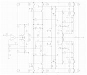
Hi Mason,Seeing here and IanHegglun's thread, I also pulled out the non-switching output prototype in the barrack state that I built two years ago from a corner of the storeroom
View attachment 1166016
Q1, Q2, Q9, and Q10 form a multiplication square root circuit. For heat dissipation and temperature tracking, these transistors are attached to another aluminum L-angle machined heatsink.
The ratio of the output stage bias current and the reference current flowing from Q1 to Q2 is determined by the ratio of the saturation currents “Is” of the C5198/A1941 and TTC004/TTA004. Since it is difficult to determine the bias current by calculation, it is possible to adjust the value of R2.
Diode-connected Q9 and Q10 deviate from the exponential function characteristics due to parasitic resistance and other factors when a large current flows.
Therefore, Icn * Icp = constant does not hold true, but it is OK as long as there is no cutoff.
Your method of having a diode in parallel with the sense resistor to hold enough current even in the off-side transistor might be a good approach.
My drive circuit (OTA?) uses the power supply current of the operational amplifier used in Alexander amplifiers etc. as an output.
The power supply voltage is limited to ±20V or less because the board of the small output amplifier that I made earlier is used and the cascode of the op amp is omitted. We plan to eventually add a cascode to allow for a larger swing.
The OPA828 I am using is very excellent and I think it is suitable for this circuit.
I like the simplicity of the circuit. Are your schematics complete? I don't see where the Imon nodes connect.
Thanks,
Hi gman76, thanks for your interest.
No particular progress, however.
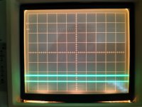
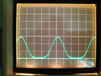
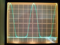
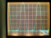
Imon is a current monitor, a test pin to observe the collector current waveform of the OPS by observing both ends of 40mΩ with an oscilloscope.
The attached picture shows the observed waveform, which is the voltage between -Vc and Imon_n. The straight bright line at the bottom is the 0V reference line. 10mV/Div means 250mA/Div.
1. when there is no signal, the bias current is about 150mA.
2. at output 2W (8Ω) 1kHz, there is a margin to the cutoff.
3. At 12.5W output, it seems to have almost reached the cutoff critical point.
4. At 12.5W 50kHz, there is a little delay in bias control.
My goal was for the OPS to operate with no cutoff, but that may be a little difficult to achieve. However, the collector current changes very smoothly compared to a typical Class AB with an emitter resistor.
I think ttlhacker's circuit will be far more marginally non-cutoff if it is operating as intended.
I am hoping the OP can present its waveform. Because I think it is the most distinctive part of his design.
No particular progress, however.
Imon is a current monitor, a test pin to observe the collector current waveform of the OPS by observing both ends of 40mΩ with an oscilloscope.
The attached picture shows the observed waveform, which is the voltage between -Vc and Imon_n. The straight bright line at the bottom is the 0V reference line. 10mV/Div means 250mA/Div.
1. when there is no signal, the bias current is about 150mA.
2. at output 2W (8Ω) 1kHz, there is a margin to the cutoff.
3. At 12.5W output, it seems to have almost reached the cutoff critical point.
4. At 12.5W 50kHz, there is a little delay in bias control.
My goal was for the OPS to operate with no cutoff, but that may be a little difficult to achieve. However, the collector current changes very smoothly compared to a typical Class AB with an emitter resistor.
I think ttlhacker's circuit will be far more marginally non-cutoff if it is operating as intended.
I am hoping the OP can present its waveform. Because I think it is the most distinctive part of his design.
Attachments
- Home
- Amplifiers
- Solid State
- Easy to compensate and stable LT1166-like wideband auto-bias amp - design and build