Hi,
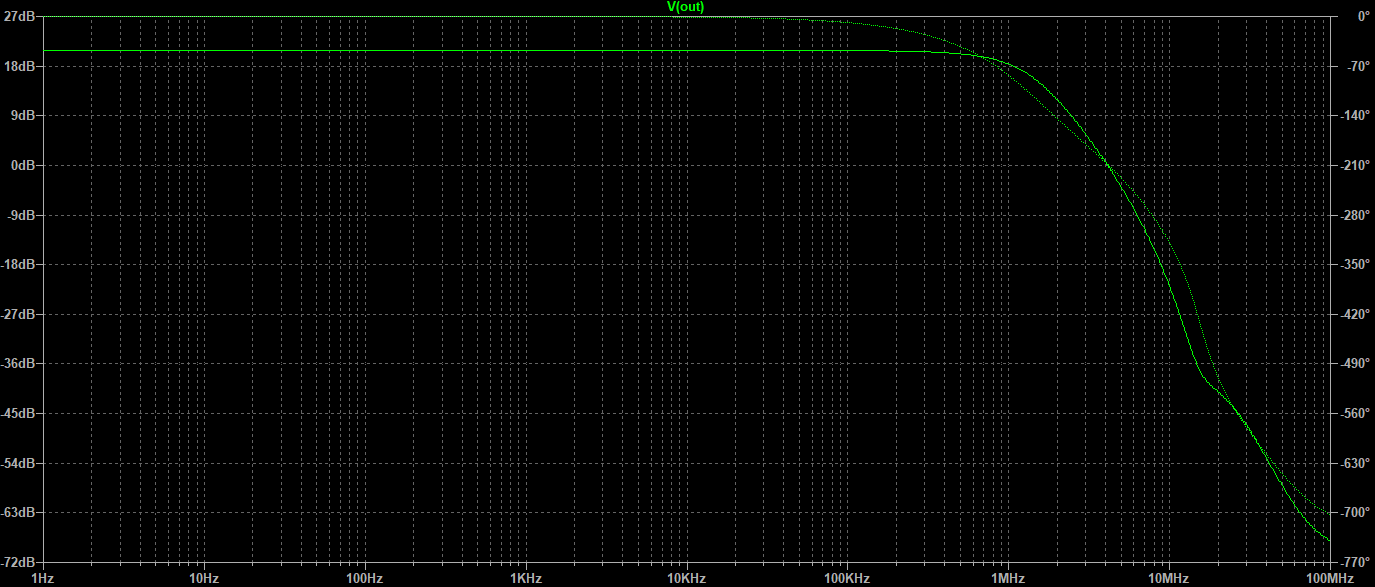
I managed to come up with an auto-bias amp topology that's easy to compensate, stable, and has high bandwidth (about 1MHz). It's similar to the LT1166 at its core but a few improvements make it much more stable and also capable of handling higher frequencies.
S
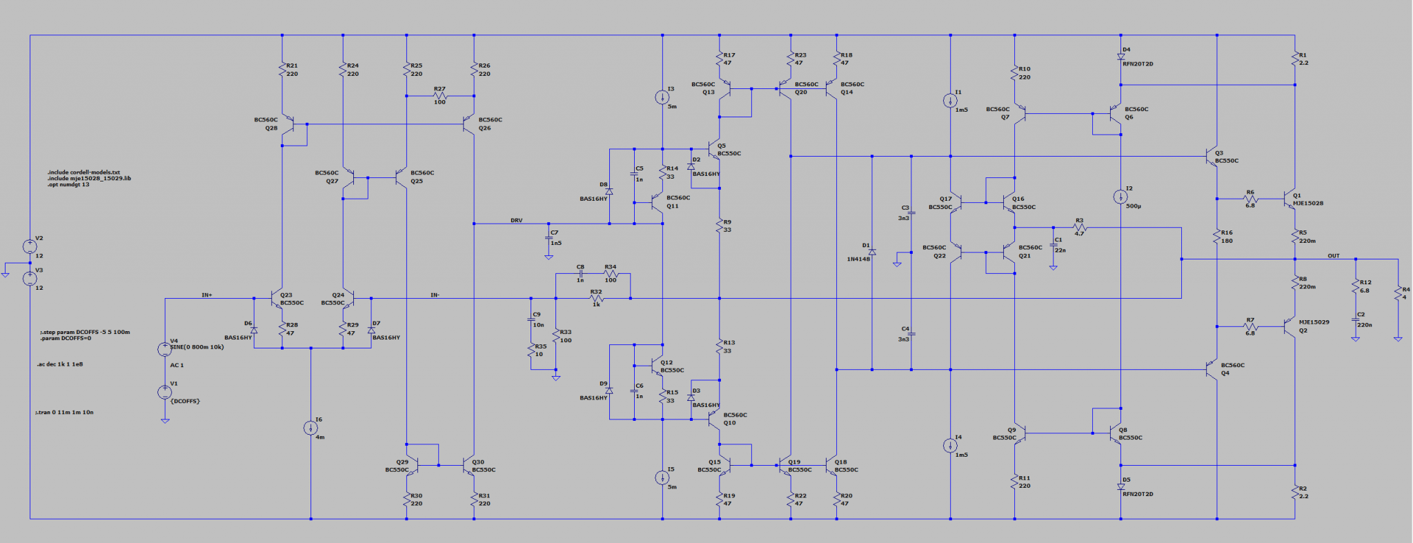 chematic:
The LTSpice ASC file is attached.
The circuit is based around the same current multiplier cell that's also found in the LT1166 (Q16/17/21/22). Unlike the LT1166, the output stage's bias current is measured at the collectors of the output transistors. A divided-down version of the output transistors' collector currents is fed into the multiplier cell via Q6/7/8/9. Deviating from the LT1166 again, the output current of the multiplier cell is fed directly into compensation capacitors C3/C4. There's no additional shunt regulator like in the LT1166, which would degrade the phase margin and frequency response of the auto-bias feedback loop.
When the amp is quiescent, the currents through both output transistors are equal. This means that the input currents to the multiplier cell are also equal, and as a result, the multiplier cell just acts as a pair of current mirrors under those conditions. Therefore, the current through R10 and R11 is equal to I1 and I4. Since R10 and R11 are 100x R1 and R2, the output stage's quiescent current will be 100x I1, or 150mA. Under load, the auto-bias feedback loop keeps the product of the currents through R1 and R2 constant, just like the LT1166.
The quiescent current is chosen so that the voltage across R1 and R2 is approximately 300mV when the amplifier is idle. This means that the parallel diodes (D4 and D5) won't conduct at the amp's quiescent point. When the amp is loaded, however, the diodes clamp the voltage across R1 and R2 to approximately 600mV. As a result, the dynamic range of the input current to the multiplier cell is quite limited: It can at most double in value. This, however, means that the current through the "inactive" half of the output stage can only drop to half the quiescent current since the multiplier cell keeps the product of its two input currents constant. The overall effect of the clamp diodes in parallel to the current sense resistors is that the current through the inactive half of the output stage never drops below about 75mA (in practice, it'll go a tiny bit lower due to the clamp diodes not being quite perfect - I observed about 60mA). The crossover is also very smooth since the product of the output transistor currents is held constant during the crossover phase (constant current product = constant Vbe sum).
Emitter resistors R5 and R8 limit the loop gain of the auto-bias feedback loop to make it easier to compensate. (Q1/R1/R5 and Q2/R2/R8 each form a common-emitter amp with G<10, making manual analysis of the feedback loop rather simple.)
Low-pass R3/C1 prevents a parasitic positive feedback path from forming through the parasitic capacitances of the multiplier cell. It is not necessary for the voltage at the emitter of Q16/Q21 to accurately track the output voltage as long as it doesn't deviate more than a diode drop at signal frequencies (hence the low value of R3).
The multiplier cell can be constructed with cheap BCM61B/BCM62B transistors, which each contain an NPN or PNP pair with tightly matched Vbe. This avoids the need to manually match and thermally couple discrete transistors for the multiplier.
The auto-bias output stage is driven by a current-feedback OTA stage to set the amp's output voltage (Q5/10/11/12 + the connected current mirrors). This OTA always injects the same current into both C3 and C4 in order to make the voltages on them slew equally. In other words, the output-voltage feedback loop (via the OTA) only uses common-mode signals on C3/C4, while the auto-bias feedback loop uses differential-mode signals on the same capacitors. As a result, even though both feedback loops share the same compensation capacitors, they can operate independently. This improves stability dramatically.
The gain of the current-feedback amplifier stage is 1. Its gain-bandwidth product can be set by adjusting R9/13/14/15. This means that the output-voltage feedback loop can still be compensated independently even though the value of C3/C4 is dictated by the auto-bias circuitry. It's also possible to use a LM13700 instead of the discrete current-feedback OTA.
Finally, a G=11 stage with global feedback all the way to the left of the schematic completes the amp. I opted for a folded-cascode configuration, but pretty much anything would work. (Yes, I know... Nested feedback loops. They're fine if you just compensate them properly, which C7 does.)
Bandwidth:
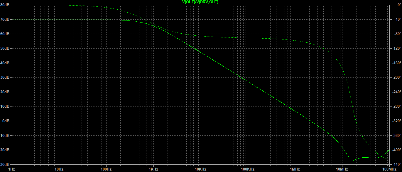
CFB OTA phase margin (almost 90°):
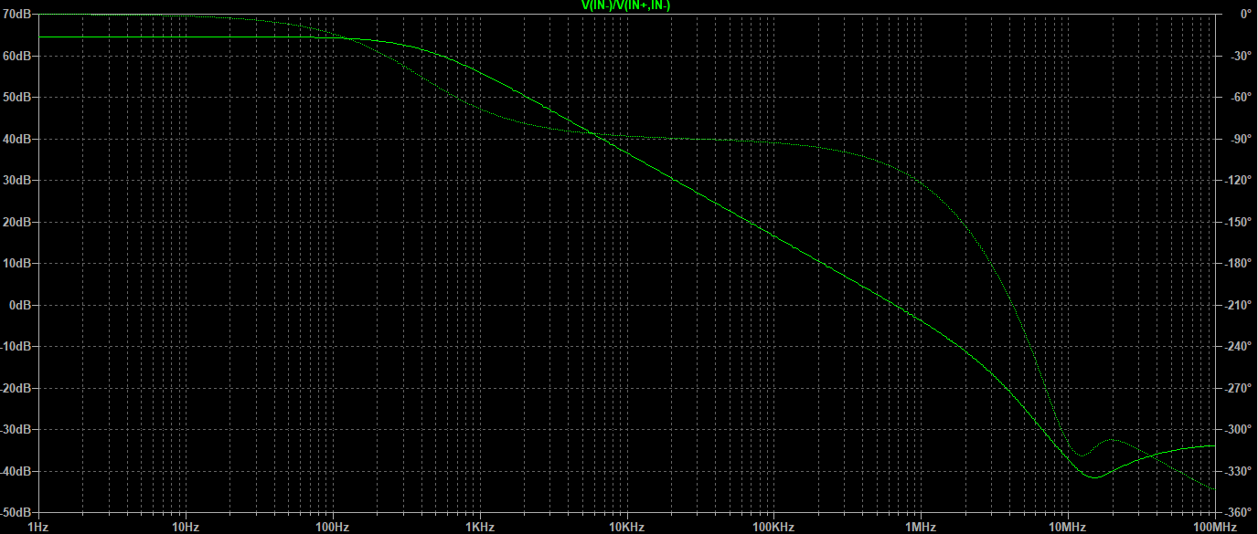
G=11 input stage phase margin (about 70°):
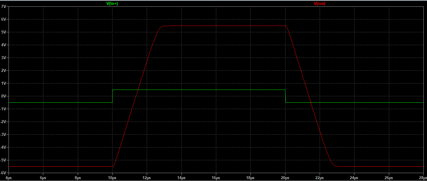
Large-signal step response (3.5V/µs output slew rate):
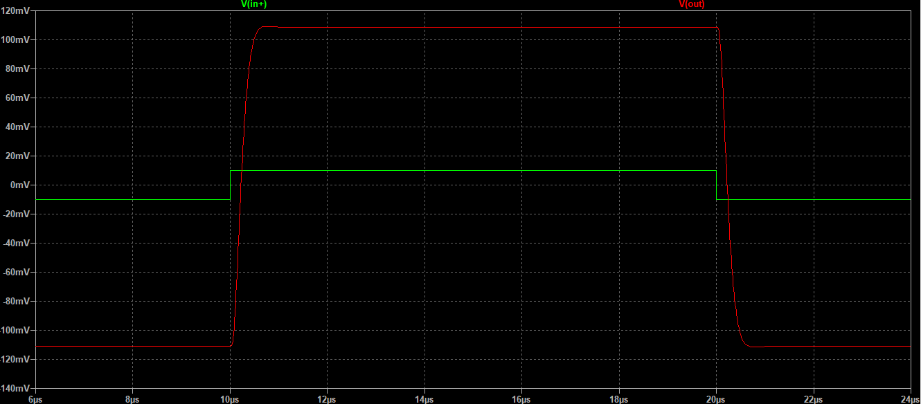
Small-signal step response:
If you have any suggestions on how I could improve this amp further, let me know!
I'm going to order parts, make a PCB layout and build this thing over the next few weeks. (I'm planning to use it as my new main amp.)
Thanks,
Jonathan
I managed to come up with an auto-bias amp topology that's easy to compensate, stable, and has high bandwidth (about 1MHz). It's similar to the LT1166 at its core but a few improvements make it much more stable and also capable of handling higher frequencies.
S
The LTSpice ASC file is attached.
The circuit is based around the same current multiplier cell that's also found in the LT1166 (Q16/17/21/22). Unlike the LT1166, the output stage's bias current is measured at the collectors of the output transistors. A divided-down version of the output transistors' collector currents is fed into the multiplier cell via Q6/7/8/9. Deviating from the LT1166 again, the output current of the multiplier cell is fed directly into compensation capacitors C3/C4. There's no additional shunt regulator like in the LT1166, which would degrade the phase margin and frequency response of the auto-bias feedback loop.
When the amp is quiescent, the currents through both output transistors are equal. This means that the input currents to the multiplier cell are also equal, and as a result, the multiplier cell just acts as a pair of current mirrors under those conditions. Therefore, the current through R10 and R11 is equal to I1 and I4. Since R10 and R11 are 100x R1 and R2, the output stage's quiescent current will be 100x I1, or 150mA. Under load, the auto-bias feedback loop keeps the product of the currents through R1 and R2 constant, just like the LT1166.
The quiescent current is chosen so that the voltage across R1 and R2 is approximately 300mV when the amplifier is idle. This means that the parallel diodes (D4 and D5) won't conduct at the amp's quiescent point. When the amp is loaded, however, the diodes clamp the voltage across R1 and R2 to approximately 600mV. As a result, the dynamic range of the input current to the multiplier cell is quite limited: It can at most double in value. This, however, means that the current through the "inactive" half of the output stage can only drop to half the quiescent current since the multiplier cell keeps the product of its two input currents constant. The overall effect of the clamp diodes in parallel to the current sense resistors is that the current through the inactive half of the output stage never drops below about 75mA (in practice, it'll go a tiny bit lower due to the clamp diodes not being quite perfect - I observed about 60mA). The crossover is also very smooth since the product of the output transistor currents is held constant during the crossover phase (constant current product = constant Vbe sum).
Emitter resistors R5 and R8 limit the loop gain of the auto-bias feedback loop to make it easier to compensate. (Q1/R1/R5 and Q2/R2/R8 each form a common-emitter amp with G<10, making manual analysis of the feedback loop rather simple.)
Low-pass R3/C1 prevents a parasitic positive feedback path from forming through the parasitic capacitances of the multiplier cell. It is not necessary for the voltage at the emitter of Q16/Q21 to accurately track the output voltage as long as it doesn't deviate more than a diode drop at signal frequencies (hence the low value of R3).
The multiplier cell can be constructed with cheap BCM61B/BCM62B transistors, which each contain an NPN or PNP pair with tightly matched Vbe. This avoids the need to manually match and thermally couple discrete transistors for the multiplier.
The auto-bias output stage is driven by a current-feedback OTA stage to set the amp's output voltage (Q5/10/11/12 + the connected current mirrors). This OTA always injects the same current into both C3 and C4 in order to make the voltages on them slew equally. In other words, the output-voltage feedback loop (via the OTA) only uses common-mode signals on C3/C4, while the auto-bias feedback loop uses differential-mode signals on the same capacitors. As a result, even though both feedback loops share the same compensation capacitors, they can operate independently. This improves stability dramatically.
The gain of the current-feedback amplifier stage is 1. Its gain-bandwidth product can be set by adjusting R9/13/14/15. This means that the output-voltage feedback loop can still be compensated independently even though the value of C3/C4 is dictated by the auto-bias circuitry. It's also possible to use a LM13700 instead of the discrete current-feedback OTA.
Finally, a G=11 stage with global feedback all the way to the left of the schematic completes the amp. I opted for a folded-cascode configuration, but pretty much anything would work. (Yes, I know... Nested feedback loops. They're fine if you just compensate them properly, which C7 does.)
Bandwidth:
CFB OTA phase margin (almost 90°):
G=11 input stage phase margin (about 70°):
Large-signal step response (3.5V/µs output slew rate):
Small-signal step response:
If you have any suggestions on how I could improve this amp further, let me know!
I'm going to order parts, make a PCB layout and build this thing over the next few weeks. (I'm planning to use it as my new main amp.)
Thanks,
Jonathan
Attachments
Thanks a lot!Interesting design sir. My hat off.
Here's the simulated distortion spectrum at 1kHz, 1Vpp input (11Vpp output into 4 Ohms):
And at 10kHz, same amplitude, same load:
I'm still tweaking the compensation scheme slightly (trying to block all potential >10MHz parasitic feedback paths); I'll post an updated version of the schematic soon (and hopefully also a board layout).
This auto-bias scheme seems to work quite well for reducing THD, probably because it's fast enough to keep the bias tightly regulated even at >10kHz, avoiding crossover altogether.
The THD of the final physical amp will probably just depend on the quality of the board layout. It'll be a bit simpler than most other amps, though, since there is no classical VAS and all compensation capacitors return to the (hopefully) clean ground. (PSRR should therefore be pretty good too.)
The initial version of the amp will also just be for +/-12V or +/-15V operation with a 4 Ohm load. I don't need much power. That's also why I chose the CFB OTA and folded cascode configurations - they allow the output of the amp to swing rather close to the supply rails.
Parts are ordered now!
Hi Jonathan,
I found compensation can be improved for 20kHz by reducing C3,C4 across the bias generator and a series resistor to reduce ringing. My sim files are attached.
Below shows the original C3,C4 at 20kHz with a triangle wave:
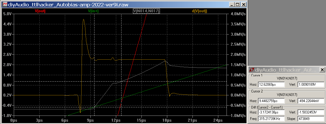
The blip in "d(Vout)" gain at 12us is due to the bias generators delay to start working with Vin increasing - because C3,C4 is too large.
With C3,C4 reduced to 1nF and 47R series resistor fixes this at 20kHz as below:
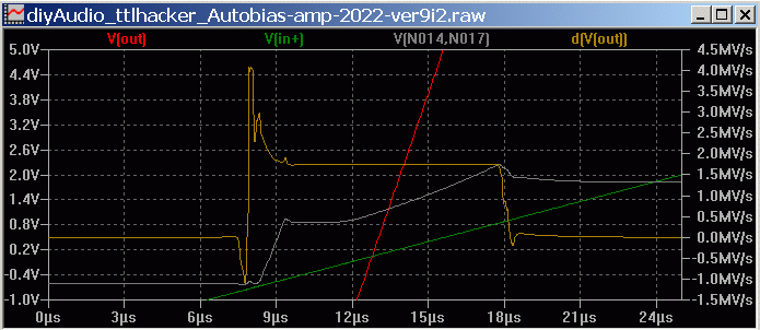
Notice the blip at 12us has gone. The series resistor needs to be minimised as too large value will causes continuous oscillation. Too small and there is ringing eg at 8us. BTW The plot of V(N014,N017) is the base-emitter voltage of bias generator Q17 - it shows when the bias generator is active, here from 10us to 18 us. It stop/starts at 10us giving a gain blip.
I was interested to see the crossover distortion at 20kHz and whether it changes much going from 1kHz to 20kHz?
The plot below shows the crossover region at 20kHz:
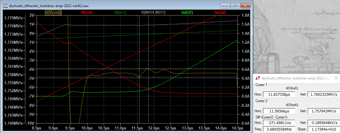
The amount of crossover distortion at 20kHz is related to the change in gm over the crossover region, here the change in gm is about 0.2% at 20kHz. This gives something in the range of 0.01% THD.
At 1kHz (below) the gain change in the crossover region is almost the same:
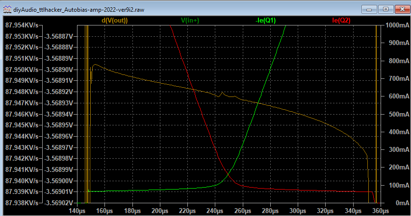
At 1kHz the crossover gain wiggles are on top of gm ramping down which represents mainly 2nd Harmonic distortion (which is less audible than higher order products from the crossover region).
As for the difference between 1kHz and 20kHz crossover distortion -- it appears to be about the same -- because the gain change in the crossover region is almost the same at 20kHz as 1kHz. This shows the autobias loop is operating "wideband" at least up to 20kHz. (Typically, the standard topology crossover distortion usually significantly increases going from 1kHz to 20kHz).
This design appears to offer a significant improvement over standard topology biasing in terms of reducing crossover distortion over the full audio range.
Again congratulations.
Congratulations on a wideband autobias design!If you have any suggestions on how I could improve this amp further, let me know!
I found compensation can be improved for 20kHz by reducing C3,C4 across the bias generator and a series resistor to reduce ringing. My sim files are attached.
Below shows the original C3,C4 at 20kHz with a triangle wave:
The blip in "d(Vout)" gain at 12us is due to the bias generators delay to start working with Vin increasing - because C3,C4 is too large.
With C3,C4 reduced to 1nF and 47R series resistor fixes this at 20kHz as below:
Notice the blip at 12us has gone. The series resistor needs to be minimised as too large value will causes continuous oscillation. Too small and there is ringing eg at 8us. BTW The plot of V(N014,N017) is the base-emitter voltage of bias generator Q17 - it shows when the bias generator is active, here from 10us to 18 us. It stop/starts at 10us giving a gain blip.
I was interested to see the crossover distortion at 20kHz and whether it changes much going from 1kHz to 20kHz?
The plot below shows the crossover region at 20kHz:
The amount of crossover distortion at 20kHz is related to the change in gm over the crossover region, here the change in gm is about 0.2% at 20kHz. This gives something in the range of 0.01% THD.
At 1kHz (below) the gain change in the crossover region is almost the same:
At 1kHz the crossover gain wiggles are on top of gm ramping down which represents mainly 2nd Harmonic distortion (which is less audible than higher order products from the crossover region).
As for the difference between 1kHz and 20kHz crossover distortion -- it appears to be about the same -- because the gain change in the crossover region is almost the same at 20kHz as 1kHz. This shows the autobias loop is operating "wideband" at least up to 20kHz. (Typically, the standard topology crossover distortion usually significantly increases going from 1kHz to 20kHz).
This design appears to offer a significant improvement over standard topology biasing in terms of reducing crossover distortion over the full audio range.
Again congratulations.
Attachments
Last edited:
Hey, thanks a lot!Hi Jonathan,
Congratulations on a wideband autobias design!
I found compensation can be improved for 20kHz by reducing C3,C4 across the bias generator and a series resistor to reduce ringing. My sim files are attached.
I already knew that the auto-bias was getting slightly sluggish at 20kHz, but haven't "dared" to include series resistors with the compensation capacitors yet. Now that I think about it, though, it does make perfect sense. The bias control loop has well-defined gain (independent of its current operating point) due to the emitter resistors in the output stage and the fact that the rest of it is just current mirrors. So, if you insert resistors in series with the compensation caps, they just have to be small enough to keep the gain below 1 at high frequencies for stability... Nice! I'll have to check how the CFB OTA behaves with the added resistors, but it shouldn't be any different there. Maybe I could add another 100pF cap or so (without a resistor) to rule out high-frequency oscillations.
One thing I did in the simulation to make sure the auto-bias loop is stable is to attach a squarewave current source to the amp's output, switching between 1A and -1A with 1µs rise and fall time. This causes the auto-bias loop to slew rapidly, and the ringing (or absence thereof) as the new bias settles is a very nice indicator of proper loop compensation. 3.3nF gave me the nicest settling, but I'll do the same thing again with your suggested changes.
On the other hand, though, nobody's going to drive the amp with a 20kHz full-range sinewave anyway, and the autobias still works properly at >50kHz. At lower amplitudes, the auto-bias feedback loop is plenty fast to keep the distortion super low even at 20kHz and above. But I might just as well include the footprints for your suggested compensation scheme on the PCB anyway; that way I can test both schemes.
My main goal for the amp was to make it wideband, but with rock-solid compensation and biasing, so I went with bigger phase margins than would've technically been necessary. I'm sure THD performance could get quite a bit better still if you pushed the amp closer to the edge - but before I try that, I want it to operate reliably. (Also, this is just going to be the amp for my computer speakers... Sliiiight overkill...)
In any case, thanks a lot for the compliments!
Parts are slowly arriving, so I'll start prototyping over the next few days.
Hi Jonathan,
You may be interested to see I have modified your interesting autobias approach to allow high voltages while using only low voltage small signal transistors.
I have posted it in my thread here since I assume your amp is almost up and running. Looking forward to hearing how it goes.
You may be interested to see I have modified your interesting autobias approach to allow high voltages while using only low voltage small signal transistors.
I have posted it in my thread here since I assume your amp is almost up and running. Looking forward to hearing how it goes.
Thank you all so much! 
"Almost up and running" isn't quite true, sadly - the complexity of the beast I came up with is insane... I'm trying to fit a stereo amp with output protection onto a single 160x100mm board, which is proving to be rather difficult, but I'm getting there. I'd like this amp design to be both a testbed for new feedback loop ideas and the main amp for the (low-power) speakers at my desk. That's why I'm going for a modular approach: Output transistors on a base board, autobias + CFB OTA on a plug-in module, and the input stage on another module. That way I can just swap modules if the compensation scheme doesn't work, for example. I've also added space for an input module (for Toslink, which I'll need once the amp works), a speaker protection module, and a power input module (which can house some isolated DC/DC converters).
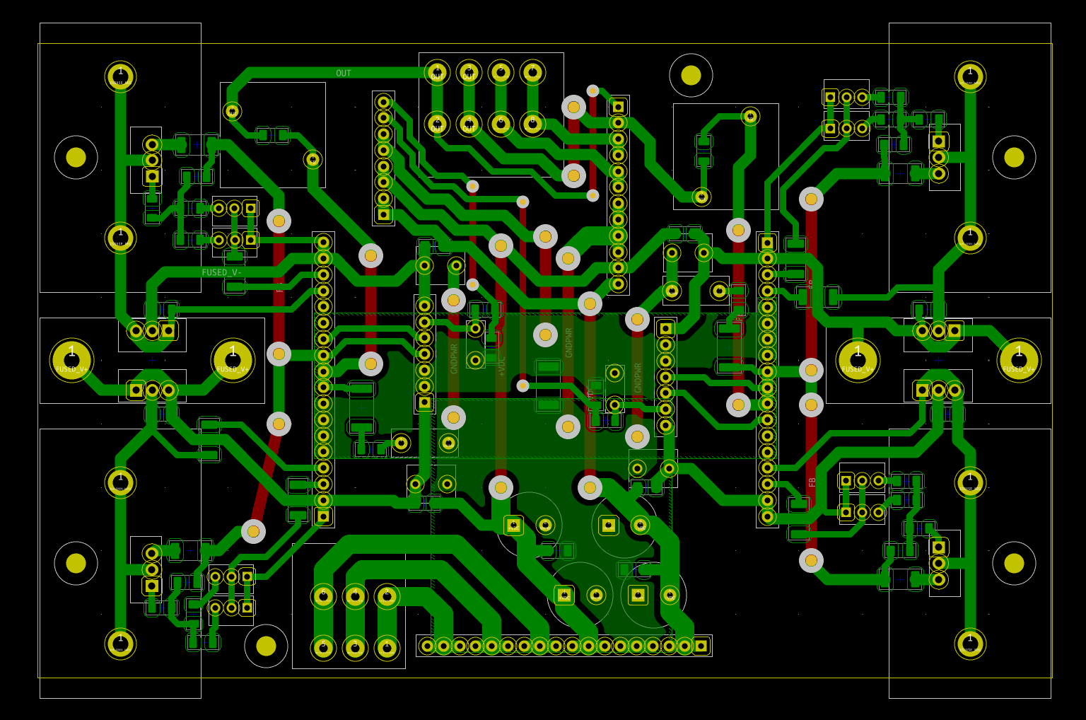
The layout of the base board currently looks like this (single layer, with star grounding and separate power/signal grounds):
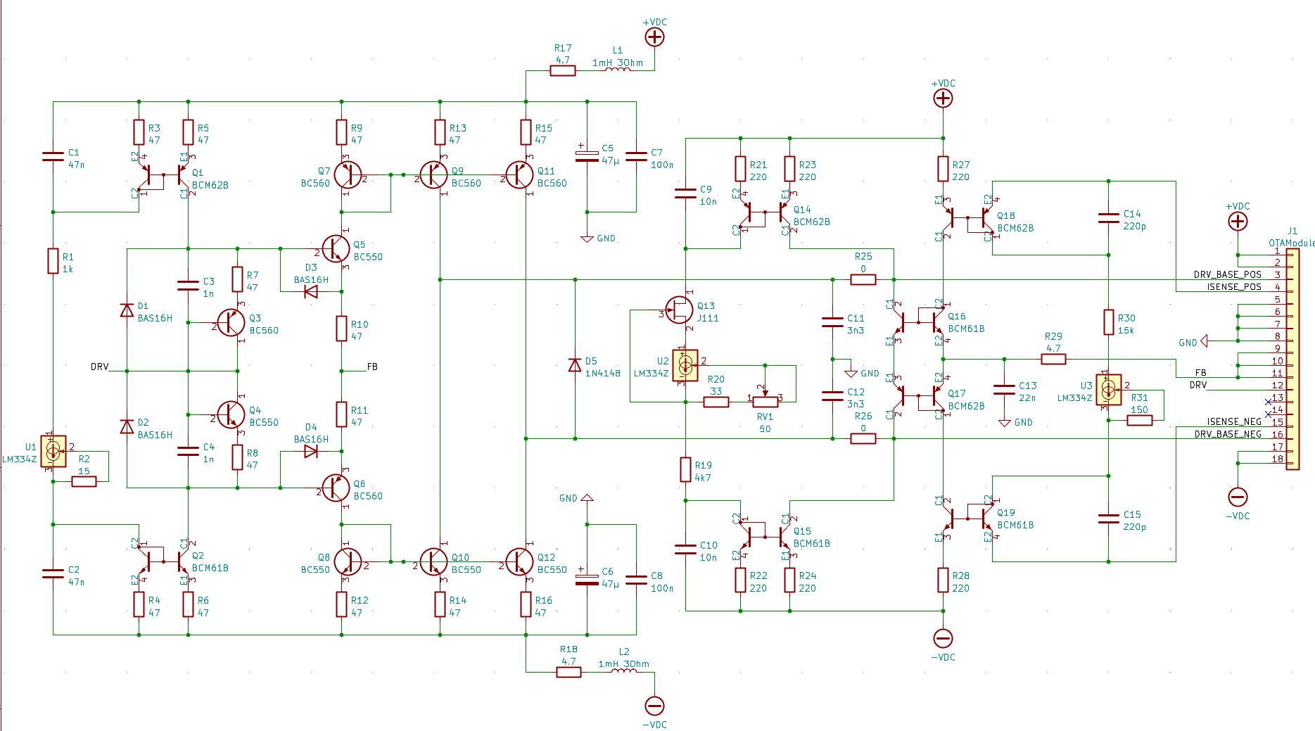
And right now I'm finishing up the schematic of the OTA module:
I'll get back to you soon when I have layouted all of the important modules! (OTA module + Input LTP module)
Oh, and I've also realized that if you place the damping resistors for the autobias compensation caps as shown in the schematic above (R25/R26, 0 Ohm placeholders for now), you can dampen the autobias feedback loop without influencing the OTA feedback loop at all. (If you just add them in series with the caps, the gain margin of the OTA degrades dramatically.)
I've originally had the sense resistors on the emitters too. However, I found that that made the phase margins of the various feedback loops slightly worse since high-frequency oscillations (tens of MHz) could couple directly from the output back into the multiplier cell. That's why I moved the current sense resistors to the collectors and introduced an RC low-pass in the emitter connection of the multiplier cell. Only then could I eliminate all peaking in all of the amp's many feedback loops. I'm really quite curious to see if this simplified version is stable too, though!Hi Jonathan,
You may be interested to see I have modified your interesting autobias approach to allow high voltages while using only low voltage small signal transistors.
I have posted it in my thread here since I assume your amp is almost up and running. Looking forward to hearing how it goes.
"Almost up and running" isn't quite true, sadly - the complexity of the beast I came up with is insane... I'm trying to fit a stereo amp with output protection onto a single 160x100mm board, which is proving to be rather difficult, but I'm getting there. I'd like this amp design to be both a testbed for new feedback loop ideas and the main amp for the (low-power) speakers at my desk. That's why I'm going for a modular approach: Output transistors on a base board, autobias + CFB OTA on a plug-in module, and the input stage on another module. That way I can just swap modules if the compensation scheme doesn't work, for example. I've also added space for an input module (for Toslink, which I'll need once the amp works), a speaker protection module, and a power input module (which can house some isolated DC/DC converters).
The layout of the base board currently looks like this (single layer, with star grounding and separate power/signal grounds):
And right now I'm finishing up the schematic of the OTA module:
I'll get back to you soon when I have layouted all of the important modules! (OTA module + Input LTP module)
Oh, and I've also realized that if you place the damping resistors for the autobias compensation caps as shown in the schematic above (R25/R26, 0 Ohm placeholders for now), you can dampen the autobias feedback loop without influencing the OTA feedback loop at all. (If you just add them in series with the caps, the gain margin of the OTA degrades dramatically.)
Hi Jonathan,
Maybe I need to try 5GHz mirrors versus BC61/62's in my modified version to see if there is a need for faster autobias mirror transistors? But I have another build on the go at present.
That's interesting that you have tried a few other options. Another option might be to use 5GHz transistors in the autobias loop mirrors. EG the BFR96 series (NPN) and BFQ32 (PNP) series. These are not as easy to sourced as the BC61/62 series. The 5GHz PNP's are rarer than the 5GHz PNPs; for PNP's search for BFQ19, BFQ32S, BFQ54T, BFQ79, BFT96, BFQ194. Unfortunately all these are only 15V devices so may not be an option in most amp designs. In my modified version this is not a problem since I use a +/-5V auxiliary supply for all the autobias transistors.I've originally had the sense resistors on the emitters too. However, I found that that made the phase margins of the various feedback loops slightly worse since high-frequency oscillations (tens of MHz) could couple directly from the output back into the multiplier cell. That's why I moved the current sense resistors to the collectors and introduced an RC low-pass in the emitter connection of the multiplier cell. Only then could I eliminate all peaking in all of the amp's many feedback loops. I'm really quite curious to see if this simplified version is stable too, though!
Maybe I need to try 5GHz mirrors versus BC61/62's in my modified version to see if there is a need for faster autobias mirror transistors? But I have another build on the go at present.
As far as I can tell, the big issue isn't necessarily the transition frequency, it's the parasitic capacitances of the small-signal transistors. These allow extremely high frequency signals to take paths through the circuit that you'd not usually expect to be feedback paths - i.e. from the bases of the multiplier cell directly to the collectors, turning negative feedback into positive feedback. Collector-base capacitance appears to be the most critical. The BCM61B and BCM62B already have a collector-base capacitance of 1.5pF/2.2pF max respectively, which actually matches that of the 5GHz transistors you mentioned - so the BCMs should already be optimal. The standard BC550C/BC560C also only have 2.5pF, and so do the BC546C/BC556C.Hi Jonathan,
That's interesting that you have tried a few other options. Another option might be to use 5GHz transistors in the autobias loop mirrors. EG the BFR96 series (NPN) and BFQ32 (PNP) series. These are not as easy to sourced as the BC61/62 series. The 5GHz PNP's are rarer than the 5GHz PNPs; for PNP's search for BFQ19, BFQ32S, BFQ54T, BFQ79, BFT96, BFQ194. Unfortunately all these are only 15V devices so may not be an option in most amp designs. In my modified version this is not a problem since I use a +/-5V auxiliary supply for all the autobias transistors.
Maybe I need to try 5GHz mirrors versus BC61/62's in my modified version to see if there is a need for faster autobias mirror transistors? But I have another build on the go at present.
Incidentally, I found that base-collector and base-emitter capacitance is also one of the primary reasons why CFB amps are often more stable than VFB ones! At very high frequencies, you get strong capacitive coupling between the LTP's common emitter node and the inverting input's base, which introduces a pole in the feedback loop's frequency response and ruins your phase margin if you push the gain-bandwidth product too high (a fact that seems to be well known). This is the reason for the unusual voltage feedback divider in my original LTSpice schematic - it uses a scheme that's similar to oscilloscope probe compensation (capacitive voltage divider) to lower its impedance at high frequencies so it can simply overpower the parasitic capacitances in the LTP. CFB amps don't have that problem since they operate as current conveyors (and again, that's the reason why I chose to design a CFB OTA to drive the output stage - the entire output stage drive circuitry, consisting of CFB OTA + auto-bias loop, is a pile of nothing but current conveyors to prevent awful high frequency poles).
I tried quite hard to eliminate all possible unwanted high-frequency feedback paths in my version of the amp to give it the best chances at actually being stable. This also made all peaking on all nodes of the entire amp disappear in the LTSpice AC simulation and it's the reason for all of those random low-value capacitors throughout the amp, which might seem unnecessary at first glance. They prevent 20+ MHz signals from going places.
The single-layer board design together with its short ground paths should also help with parasitic capacitances.
Last edited:
Hi Jonathan,
But if not then maybe lower Cbc devices eg HFA3096 array will remove the extra mirrors unwanted poles in the autobisas loop (in my modified version). I notice the HFA3096 array is available at Digikey for about $20 in Australia or $5 per transistor. Eek : at that price maybe only use it for the first mirror (my Q3/4 and Q23/24).
But since the HFA3096 is only a 12V device it's not useable in your circuit above. They would need to be cascoded, but that up's complexity. It seems autobias always has something in the path to stop us from using it .
.
I agree, at least for your version where Vce changes due to output voltage. But in my modified version (here) the Vce of the mirrors are bootstrapped using the +/-5V auxiliary supply, so themirror transistors (my Q4,Q6) Vce remains fairly constant. So these mirrors may benefit from a high FT even if their Cbc is not changed. Maybe?Collector-base capacitance appears to be the most critical. ... so the BCMs should already be optimal.
But if not then maybe lower Cbc devices eg HFA3096 array will remove the extra mirrors unwanted poles in the autobisas loop (in my modified version). I notice the HFA3096 array is available at Digikey for about $20 in Australia or $5 per transistor. Eek
But since the HFA3096 is only a 12V device it's not useable in your circuit above. They would need to be cascoded, but that up's complexity. It seems autobias always has something in the path to stop us from using it
Yuck! Those prices!But if not then maybe lower Cbc devices eg HFA3096 array will remove the extra mirrors unwanted poles in the autobisas loop (in my modified version). I notice the HFA3096 array is available at Digikey for about $20 in Australia or $5 per transistor. Eek: at that price maybe only use it for the first mirror (my Q3/4 and Q23/24).
But since the HFA3096 is only a 12V device it's not useable in your circuit above. They would need to be cascoded, but that up's complexity. It seems autobias always has something in the path to stop us from using it.
Well, it's always possible to make the amp less sensitive to Cbc! I managed to do it in my version, after all, at the expense of throwing a truckload of transistors and bypass capacitors at it. The good old KSC3503/KSA1381 are pretty fast and still have respectable Cbc despite their 300V rating, so it's likely possible to build an amp based on my original version of the topology but for +/-40V operation. I'll tackle that after the low-power MK1 version of the amp works!
The good thing is that the multiplier cell never sees any high voltages even in my design, so we can keep using the BCM61B / BCM62B there. The rest is just current mirrors, and those aren't nearly as critical as the multiplier cell! And even if we do need better mirrors, I think cascoding BCMs with discrete high-voltage transistors should work nicely.
Yay for current conveyors!
In other news, the CFB OTA layout is still giving me some trouble, but I should get done with it today!
This was quite a bit harder to layout than I thought, but... Here are the KiCAD files for the autobias amp MK1! 
The attached ZIP file contains KiCAD projects for the amp's main PCB, as well as the OTA, LTP, and power modules. It's a small +/-15V stereo design for 4 Ohm speakers. The speaker protection and Toslink input modules aren't done yet, but they're also not needed for testing the basic functionality of the amp.
I'll start manufacturing the PCBs over the next days unless there's some kind of huge issue with the layouts.
Attachments
Sorry for going silent for so long, life's been pretty busy for me over the last few months! University and work conspired to prevent me from working on the amp 
I'm back at it now though, building the last module (OTA) before I can give the first amp channel a try. I'll show pictures when all the PCBs are cleaned and everything's assembled.
I'm back at it now though, building the last module (OTA) before I can give the first amp channel a try. I'll show pictures when all the PCBs are cleaned and everything's assembled.
- Home
- Amplifiers
- Solid State
- Easy to compensate and stable LT1166-like wideband auto-bias amp - design and build