I dont fully remember but i think i was past 50mA or even beyond 100mA before my crossover distortion fully vanished.
Btw wires/traces between drivers and outputs should be as short as possible to avoid oscillation.
Btw wires/traces between drivers and outputs should be as short as possible to avoid oscillation.
Btw wires/traces between drivers and outputs should be as short as possible to avoid oscillation.
I used 6 inch wires to the output MOSFETs on a prototype design and it worked just fine.
Class D on the other hand will fail miserably if you do that.
Sold a class d amp and someone emailed saying it didnt work just clicked. Turned out they had removed themosfets from the pcb and mounted them on a heatsink on four inch wires. Of course it stopped working. Got him to put them back on the pcb and it burst into life.
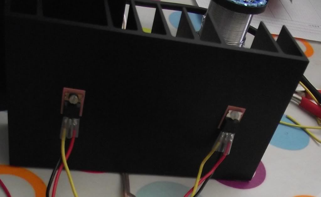
Max 2 inch. It's only to get a better placement on the heatsink. Right now they are close together. I think the heat is better dissipated if the Fets are more away from each other.
I'll take a photo to show what I mean.
I'll take a photo to show what I mean.
Its still a bad idea to have wires longer than an inch since it adds inductance to the system, increasing the risk of unstability.
Raise INDUCTANCE? It's max 22KHz, a 'coil' with an air core. Inductance won't be significant.
Like this
This is my testboard, I don't have any problems now, it's about 8cm,+3inch.
Like this
This is my testboard, I don't have any problems now, it's about 8cm,+3inch.
Last edited:
I dont fully remember but i think i was past 50mA or even beyond 100mA before my crossover distortion fully vanished.
Btw wires/traces between drivers and outputs should be as short as possible to avoid oscillation.
Agreed. At least 100mA is required to mitigate the 'transconductance droop at low Id' problem with power mosfets.
Those power mosfets have an effective Ft of 100's of MHz and at that frequency a short length of wire becomes a significant amount of inductance to cause oscillation ringing. The whole point of a gate stopper resistor is to set a low pass filter Fc much less than the frequency of the oscillator, which changes because it is based on internal dynamic components. I have witnessed short oscillation bursts >40MHz on the peaks of the signal when driving a load. The solution to this is short device pins, local compensation and closely placed decoupling caps.
You can get away with the Vbe multiplier on the pcb if you use as low a bias as possible.
I found with my IRF240/9240 design I was managing to get as low as 7mA bias without crossover distortion. With that there was no need to mount the Vbe transistor on the heatsink.
I suppose if your bias is class B then you won't run into all of those high frequency stability problems. You could just replace the Vbe multiplier with a fixed resistor too since thermal compensation is not required with class B bias. I wonder if there is an 'anti-crossover notch' at the gate pin of the mosfets with only 7mA bias.
 I guess since it does not show much at the output during a low (AF) frequency observation all the harmonics and high frequencies required are right there to fix it because that feed back loop is unlike any else in the universe and has infinite BW, does not suffer from a phase margin limitation, or IM distortions (and consequently PIM). All the feedback 'fix-it signals' are right at the gate of the mosfet in time to fix-it all.
 🙄
🙄

I demonstrated here quite a while ago the transconductance droop problem using vertical fets for class AB output stages. I modeled a simple HEC feedback/feedforward driver stage follower (much higher BW than a global loop) so that I could measure the input/output vs the error signal with different bias settings. The slope of the error signal is an indicator of the range of frequencies that is added to 'correct' for the loss of Gm in the output mosfets around the current crossing. Also to note that even at 300mA bias there is still a trace of non-linear transconductance showing. However, since Gm vs Id for these devices increases exponentially much higher bias can run into Gm doubling, creating essentially the same problems as crossover.
Raise INDUCTANCE? It's max 22KHz, a 'coil' with an air core. Inductance won't be significant.
There is more going on inside the circuit than AF frequencies. Like it or not there is RF signal energy bouncing around inside everything. How susceptible your circuit is to it helps to define it as "unconditionally stable".
The whole point of a gate stopper resistor is to set a low pass filter Fc much less than the frequency of the oscillator, which changes because it is based on internal dynamic components. I have witnessed short oscillation bursts >40MHz on the peaks of the signal when driving a load. The solution to this is short device pins, local compensation and closely placed decoupling caps.
I have seen oscilation on outputs but it was usually fixed by slowing down the VAS. The audio loop requires the speed around it to be slow enough that feedback gets back to the LTP before the output swings too far causing oscilation.
I found the oscilation problems tends to be worse with quasis, which needed a cap from C to B on the lower output driver to reduce its gain.
But by slowing down the VAS you throw away all the potential bandwidth that mosfets, particularly vertical fets can achieve. IMO, a low distortion full range amplifier with BW <200KHz is noticably more acurate sounding regarding the perceived soundstage. It was not until I began to build such fast amplifiers that I noticed, it is the main reason I choose to use vertical fets as output transistors.🙂 I built a vero-board proto-amp with them once with -3db CL gain at about 400KHz. FQP14N15 & SFP9540, one is already dis-continued I think , but similar ones are available.
, but similar ones are available.Update
YouTube - Thermal compensation with IRF610
Testing the thermal compensation and it works.
But I can't set the quiescent current higher than 60mA.
YouTube - Thermal compensation with IRF610
Testing the thermal compensation and it works.
But I can't set the quiescent current higher than 60mA.
Hi all,
I'm finally going to order the parts for multiple channels, the only thing that I don't get to work is the thermal compensation. In the video above you can see that it adjusts, but won't go higher than 60mA. I'd like to set my quiescent current to 100mA.
I'm finally going to order the parts for multiple channels, the only thing that I don't get to work is the thermal compensation. In the video above you can see that it adjusts, but won't go higher than 60mA. I'd like to set my quiescent current to 100mA.
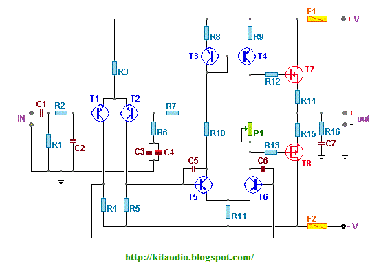
Try a slightly lower value for R19 (circuit in post#53) such as 3300 ohm. That will "turn off" the bias generator a little more allow more voltage to develop across it and turn the outputs on a little harder.
Be careful doing this as if you get it wrong very high currents could flow. Always use a bulb tester initially
Be careful doing this as if you get it wrong very high currents could flow. Always use a bulb tester initially
Try a slightly lower value for R19 (circuit in post#53) such as 3300 ohm. That will "turn off" the bias generator a little more allow more voltage to develop across it and turn the outputs on a little harder.
Be careful doing this as if you get it wrong very high currents could flow. Always use a bulb tester initially
I always put a zener across my Vbe multiplier to stop it going open circuit and blowing up the output transistors.
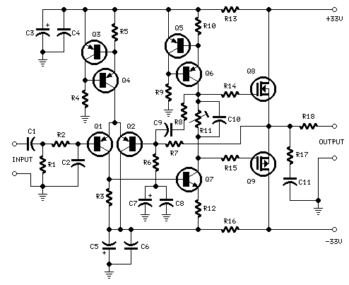
hello friends i am thinking to make this 100w amplifier using IRF540/IRF9540 can any one give reply that how amplifier is working (performence) and pcb layout
I think I've found a more reliable design
hello can any send parts list to me mail id-shravanth.reddy@yahoo.com
hello friends i have done this amp i just used +30/-30 supply for testing i have tested it. all works fine i have seted quisent current to 100ma also but R10-10k and mje340 are heating up so, please help me friends
That one will only work with lateral mosfets!
To make it your with IRF540/9540, you need to replace the pot wioth a Vbe multiplier as seen in all the bjt designs posted around here.
To make it your with IRF540/9540, you need to replace the pot wioth a Vbe multiplier as seen in all the bjt designs posted around here.
Those are also vertical mosfets and thus need the Vbe multiplier bias circuit, or thermal run away is a gurantee, unless you bias it so low that is operates in class B only.
- Home
- Amplifiers
- Solid State
- Easy and low cost: IRF540/9540 amp