2.5 amps ? I use 7ma on my irfp240/9240 amplifiers and there is no visible crossover distortion on the scope.
That's with a resistive, or a real-world load?
It seems that I can adjust the quiescent current right now
Hm, that's a bit suspicious...
You may have a 'bit' optimistic MOSFET models.
Please note that the quiscent current refers to the current of just the output pair. In order to measure it, insert a 'token' 1uohm or so resistor in the drain of one of the MOSFETs, also increase the load so that DC offset does not generate a current on the order of the quiescent current.
When your adjustment resistor is set to zero, you should have zero current. And, when it's set to 5k it should be on the order of a few amperes - so your table is wrong (perhaps the variable resistor is connected 'upside down' so the resistance reading is from the other end of the wiper - i use circuitmaker, and it does the same thing but in percentages).
While at the matter of DC offset - R2 also figures as the input resistor, in series with the 47k. Therefore your series feedbavk resistor should be more like 51k or so for close to zero DC offset.
IRF610 should of course be closely thermally coupled with the output MOSFETs - perhaps best on the ehatsink right in the middle, or even upside-down tab-on tab (insulated of course) on one of the output MOSFETs.
One thing you might want to consider is cascoding the driver stage. It is highly desirable to have a rather high current in the driver/VAS - 10s of mA come in handy. Unfortunately, this requires a rather high current from the input differential or a very high gain in the VAS transistor, which for transistors capable of operating at said currents, may be a problem. Instead, to get the high gain and high current without special transostors or a lot of dissipation in high-gain nominally small signal transistors, you can use a cascode - say BC546 under the BD139. A very small Vce is enough here - a LED from -V to the base of the BD139, fed by the base resistor for the BD140 current source (resistance properly adjusted, of course) will do the trick with minimum extra parts. Then increase the current in the VAS by about the ratio of the gain of the BC546 and BD139 to keep the currents in the input diff the same, and of course, use heatsinks on the BD139/140. Altogether that should make a very nice amp.
I am blind, dumb and stubborn and I just follow what the author says but the circuit works and for a long time.
Brian, I guess you did not ask the author for comment on the bias problem. He explain quite clearly to me. Of course you can make simple things more complicated. First you said you want a simple circuit and then you keep adding this, adding that.....making it more complicated and alien to the original. Why can you just solder this simple circuit and let it run. It is not going to cost you too much for a simple circuit like this even if it blows up right at the time you switch it on (and it is not going to do that if you had done things right) The time you spend talking on this is surely going to cost you way over the parts used. I can almost quarantee that you couldn't fail on this. (If you do, it is because you had made a mistake). You have tried the higher power version already why you doing things backwards and want to try the lower power version?
But of course you cannot expect it to be very "Hi Fi" but it is well worth for its simplicity.
I don't know why so many people hate this design. This was my door to the world of amp. diying and I will not turn my back against it.
BTW I have boards for this simple but workable circuit. Anyone interest please call. (sorry, not without charge)
tony_chan_cf@email.com
BP
First you said you want a simple circuit and then you keep adding this, adding that.....making it more complicated and alien to the original. Why can you just solder this simple circuit and let it run.
BP
I think there is a happy medium.
A design that isnt so simple it has problems but not a design that has a massive numbers of components.
I went for a design with LTP with CCS and CM.
The VAS stage has a Vbe multiplier and CCS.
This works and sounds very good.
...But of course you cannot expect it to be very "Hi Fi" but it is well worth for its simplicity.
Well said.
 A learning project? Is not the goal of a learning project to improve the system?
A design that isnt so simple it has problems but not a design that has a massive numbers of components.
I think the number of components to failure ratio has much to do with the designer.🙂
Last edited:
My IRF9240/240 amp has too much power to be used for my bookshelf speakers.
I'm using it to power a subwoofer. It is just made with protoboard so not really a professional look.
Now I want something that has about 30W and this fills my needs. I like the sound of the IRF9240/240 amp more then my Yamaha reciever, so I'm going to use my Yamaha for surround and this IRF9540/640 amp for stereo.
And yes, I want to improve my knowledge more, so a bit more complexity like a thermal compensation is no problem.
But I like the KIS principle, keep it simple. More components can cause more problems, more time to find the problems and solve them. But an amplifier needs to be stable, or not? The thermal compensation are just 2 extra components, not really a problem.
And yes, the pot was the other way around, but doens't makes any difference anyway.
bigpanda, what problems are you talking about?
bigpanda, what problems are you talking about?
I am now working on the PCB lay out.
Now I have 2 questions:
Should I use drain resistor like 0.33ohm?
My other amp uses them. I don't really know what they do, I read something about current sensing resistors.
Another question is grounding.
The designer said that you need to make 2 seperate grounds and connect then in the PSU. Why?
Now I have 2 questions:
Should I use drain resistor like 0.33ohm?
My other amp uses them. I don't really know what they do, I read something about current sensing resistors.
Another question is grounding.
The designer said that you need to make 2 seperate grounds and connect then in the PSU. Why?
If the output transistor heats up then it conducts more which heats it up even more and it can run away.
The resistors have a negative feedback effect. The more current the more the voltage across the resistor rises and shuts off the transistor a little.
The resistors have a negative feedback effect. The more current the more the voltage across the resistor rises and shuts off the transistor a little.
If the output transistor heats up then it conducts more which heats it up even more and it can run away.
The resistors have a negative feedback effect. The more current the more the voltage across the resistor rises and shuts off the transistor a little.
But also lower efficiency? So I can leave those away I guess since I'm using the IRF610 to adjust quiescent current
But also lower efficiency? So I can leave those away I guess since I'm using the IRF610 to adjust quiescent current
I would definitely add the resistors for some thermal feedback.
The irf610 on its own might not track perfectly on its own.
The only time you can skip the resistors is if you are using lateral mosfets and they have their own internel thermal feedback.
Don't you mean source resistors? Otherwise known as ballast resistors. They allow you to measure the output bias current without inserting an ammeter into the circuit. V/R=I.🙂 They also help with thermal compensation by providing a small about of local feedback by degeneration as Nigel is referring. You will find these to be necessary.I am now working on the PCB lay out.
Now I have 2 questions:
Should I use drain resistor like 0.33ohm?
My other amp uses them. I don't really know what they do, I read something about current sensing resistors.
Another question is grounding.
The designer said that you need to make 2 separate grounds and connect then in the PSU. Why?
When laying out the PCB be sure to keep 'dirty' gnds separate from 'clean' gns. Dirty gnds are those with large fluctuating currents such as the return from the filter caps, transfo center tap, or the speaker load. Clean gnds are the signal gnd reference, labeled common in RCA single end sources. Use a 'star' gnd or 'star on star' topology. A search will probably turn up a few discussions about this. Also you don't want to have large current tracks next to signal traces, especially with the higher impedance nodes.
I've tried to figure out which grounds are clean or dirty.
Actually the designer said this
Only the output (C11) needs to be grounded seperatly.
What is the difference between connecting ground on the amplifier PCB or in the PSU? It connects anyway.
An externally hosted image should be here but it was not working when we last tested it.
Actually the designer said this
A correct grounding is very important to eliminate hum and ground loops. Connect to the same point the ground sides of R1, R4, R9, C3 to C8. Connect C11 to output ground. Then connect separately the input and output grounds to power supply ground.
Only the output (C11) needs to be grounded seperatly.
What is the difference between connecting ground on the amplifier PCB or in the PSU? It connects anyway.
Think of currents flowing, you do not want to share ground paths combinging low and high current traces... ground is not dead, just as much current flows there as anywhere else.
there is a difirence between shareing a point and shareing a trace...
there is a difirence between shareing a point and shareing a trace...
What is the difference between connecting ground on the amplifier PCB or in the PSU? It connects anyway.
Don't know if this will help you or not but read it all...
http://www.diyaudio.com/forums/solid-state/101321-3-stage-lin-topology-nfb-tappings.html
Think of currents flowing, you do not want to share ground paths combinging low and high current traces... ground is not dead, just as much current flows there as anywhere else.
there is a difirence between shareing a point and shareing a trace...
Thats quite a good way of putting it.
When I look at a circuit and PCB layout now, I see it in terms of conductors with resistance. And I ask myself what can actually flow in that line or PCB track, what connects to it and where, and can that current develop a volt drop that will in any way affect the out.
When you start thinking like that and working it all out yourself rather than just following the "connect this here and that there" approach it suddenly all makes much more sense.
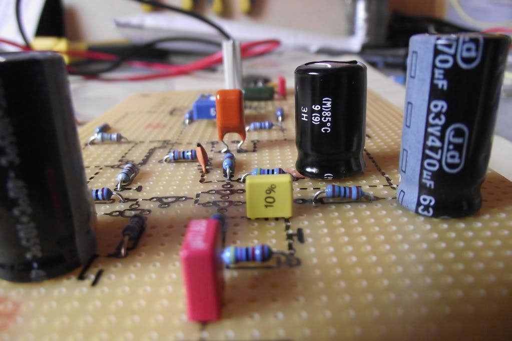
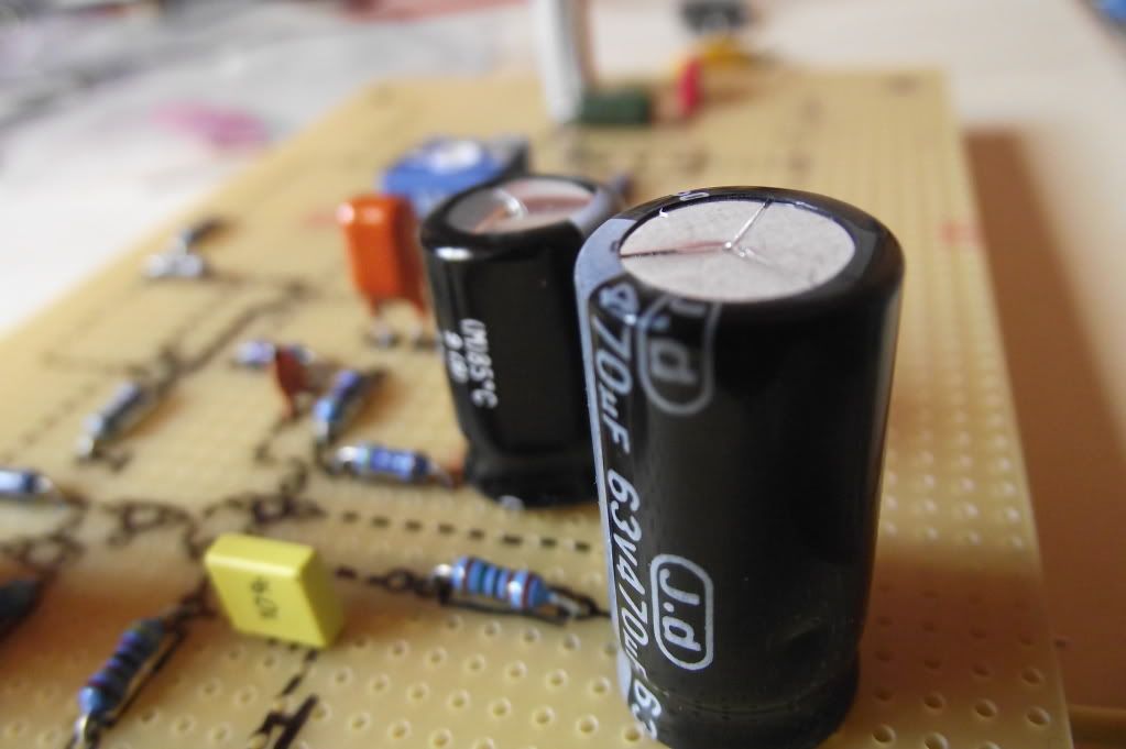
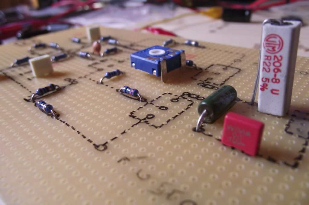
I just ordered the components for 1 channel. I'm going to solder it all to a protoboard, do some measurements, try to improve things. And most important, listen to it.
How should I mount the temperature sensing Fet on the heatsink? Right on top of an output transistor of in between the two?
How should I mount the temperature sensing Fet on the heatsink? Right on top of an output transistor of in between the two?
It seems that the amp is VERY sensitive to noise.
I have to play loud otherwise the only thing you hear is noise and clicking noises, very strange. Grounding is one big antenna right now.
From every point where a ground needs to be, a wire is connected, then all wires are connected on PSU. The wires are 30cm long right now.
But it works 🙂
I have to play loud otherwise the only thing you hear is noise and clicking noises, very strange. Grounding is one big antenna right now.
From every point where a ground needs to be, a wire is connected, then all wires are connected on PSU. The wires are 30cm long right now.
But it works 🙂
Long wires around the input can get noisy. As you say: antenna wires
Congratulations it works. Well done.
Congratulations it works. Well done.
YouTube - Mosfet IRF9540/640 Amplifier
Tomorrow I will make the ground wires as short as possible, and there is a problem with the Vbe multiplier too. I think it works in pure class B (cracks at low SPL), sound better at high SPL.Thursday I'll do some test with scope.
Tomorrow I will make the ground wires as short as possible, and there is a problem with the Vbe multiplier too. I think it works in pure class B (cracks at low SPL), sound better at high SPL.Thursday I'll do some test with scope.
- Home
- Amplifiers
- Solid State
- Easy and low cost: IRF540/9540 amp