Found the culprit..... Q608 (bd139).
I decided to try substituting every remaining transistors (Q602/604/606/608) with new ones in case one of them would have a problem when warm (they all measure well when cold). And bingo, first try, found it, new Q608 and the bias is not collapsing anymore (after 40min uptime)
I decided to try substituting every remaining transistors (Q602/604/606/608) with new ones in case one of them would have a problem when warm (they all measure well when cold). And bingo, first try, found it, new Q608 and the bias is not collapsing anymore (after 40min uptime)
Well, it was a bit too early to rejoice..... Now it's the left channel burning.....
I let the amp play music (on the light bulb tester) for more than 1 hour without any trouble.
I then tested it on my speakers and on main, but after 30min no more left channel, right channel perfectly happy.
Maybe Q607 bd139 was also defective but not as much as on the right channel so it died after a longer amount of time. I ordered 44new parts so i'll have to wait to pursue the repair
The only way to truly test a transistor is with a curve tracer but almost nobody would have one of these. Where I worked during the 80s they had a very expensive Tektronix curve tracer and it was quite amazing how may transistors which tested fine with a meter failed on the curve tracer. Usually the failure mode was breakdown as VCE was increased. Behaving a bit like a zener diode. So without a curve tracer to check transistors, I replace any that I deem remotely suspect. If an amp has had a major blowup I always replace the driver transistors also. Even if they test ok with a meter. Monitor the output with your oscilloscope while in dim bulb mode also. Looking for any oscillation at high frequency.
if you have a thermal imaging camera you can use it to find the suspect component
you can also spray the component with isopropyl alcohol and find the hot spot
you can also spray the component with isopropyl alcohol and find the hot spot
The only way to truly test a transistor is with a curve tracer but almost nobody would have one of these. Where I worked during the 80s they had a very expensive Tektronix curve tracer and it was quite amazing how may transistors which tested fine with a meter failed on the curve tracer. Usually the failure mode was breakdown as VCE was increased. Behaving a bit like a zener diode. So without a curve tracer to check transistors, I replace any that I deem remotely suspect. If an amp has had a major blowup I always replace the driver transistors also. Even if they test ok with a meter. Monitor the output with your oscilloscope while in dim bulb mode also. Looking for any oscillation at high frequency.[/QUOTE
Iam using peak electric UK semicon analyzer/ testor .Does the job. If i connect laptop i can get the family of curves ( i have not tried that yet)
Well I received the transistors.
I replaced every single transistors on both channels (power section) with rand new ones:
BD237/238 in place on 2n6551/6554, new bd139 for Q607/608 and Q609/610, new BC559B for Q603/604, new BC556B for Q605/606 and finally BC550A in place of 2sc1400 (Q601/602) I also changed power fets 2N3055/MJ2955.
I was able to set bias to 30mV through the 1R res (R653/654) without trouble (as always). All of this was made on the light bulb tester witch remained totally dimmed.
Then I shorted both 1R resistors and turned the amp on to set the offset, still with the light bulb tester.
After say 5 to 6min, the light bulb started to light up very slowly, I turned off as soon as the filament was getting red. I tried looking at the signal curve with my scope (connected to amp outputs, without load) and nothing to note at 100mV scale (AC coupling), the signal is flat.
Is the fact that the lightbulb start glowing be considered normal (Bias getting hotter) or is it the sign of potential catastrophic outcome? I would better not fry more transistors.
This circuit (as some others) use a dc feedback through what is considered a ac feedback only. The current flowing out of Q601 (only left channel notation used) is going through R635 to be 'swallowed' by Q617. VR5 is for nulling the output.
As R635 has been lowered from 2k2 to 1k2, Q601 stabilises at a different dc point. This could have consequences for C615 (1000u6.3) if the node of Q601 emitter turns negative. Check the Vdc on this cap! It can hold a reverse polarity for a short while, but will break after, say, a few minutes. A nonpol of 1000u is a bit unrealistic.
If your aim is to decrease the gain, you better increase R631 from 27E to 47E.
With these dc-stabilising topology, I would not recommend to change R635.
Use the suggested small TO92 replacements (mimicing-burning as 3055/2955) to find out dc setpoints throughout the circuit. VR5 is setting the current source as load of Q601, which makes it a very sensitive combination with the Sziklai voltage amplifier stage and its bootstrapped load of R649-C625(*)-R637.
(*) C625 is 47u25. Better us 47/63 as a minimum. If things go wrong, it will sweat.
Addendum:
I've redrawn the circuit in a more logical view, showing clearly both the dc- and ac-paths, loops and feeds. Drawings as in #1 are very confusing made by lazy designers with lack of will and paper. I shall follow your postings earnestly to get this clear.
I've redrawn the circuit in a more logical view, showing clearly both the dc- and ac-paths, loops and feeds. Drawings as in #1 are very confusing made by lazy designers with lack of will and paper. I shall follow your postings earnestly to get this clear.
If the bias drifts (having some clip leads to hook up to your newly installed emitter resistors would be handy now), verify that all of the bias spreader (Q609/610), drivers and outputs have good thermal contact to the heatsink. You did clean off the old thermal paste thoroughly, right?
I'm a bit down there, I thought that I've finally saved that amp as it has played music for hours last week without any problems, then today, right channel fried after 4minutes from cold........ I don't know where else to look for....😕
In the original drawing in post #1, the dc voltages across the circuit are shown in the lower half channel, but almost impossible to read. Can you supply me the right values? Then I can calculate various setpoints in the circuit and deduce where it might go wrong.
Have you checked the dc voltage on C615/616? These are important!
And is a drawing of the power supply available too?
Have you checked the dc voltage on C615/616? These are important!
And is a drawing of the power supply available too?
Last edited:
I've send cowneko a pm about this issue and my analysis of the circuit.
In short: my opinion about this design and NAD's commercial enterprise don't run on the same track.
W.D.E.
In short: my opinion about this design and NAD's commercial enterprise don't run on the same track.
W.D.E.
MarsBravo, thanks a lot for your dedication in helping me stabilize this amp, It's a friend amp so I cannot simply dump it away (I already have my share of good working amps, self made Pass amps, some early Sansuis...Etc), and from a simple challenge point of view, I refuse being unable to get this amp back to life (now it just seems like It enjoys suicide)
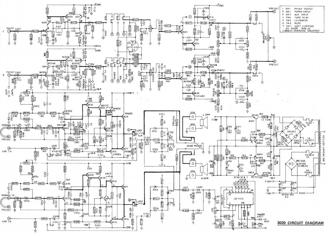
So to make things clear about my amp, here is the official schematic:
Then Here the amp I got before any modifications (seems like all differences are from manufacturer but I can't be sure (especially for the power bjts)
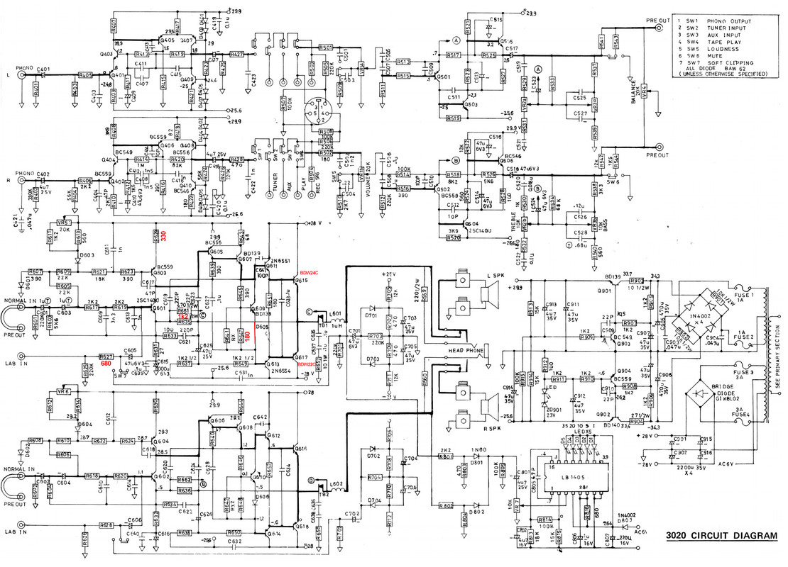
some resistors value have changed, a diode has been removed and replaced by a jumper wire and the 2n3055/MJ2955 have been replaced with BDW22C/24C
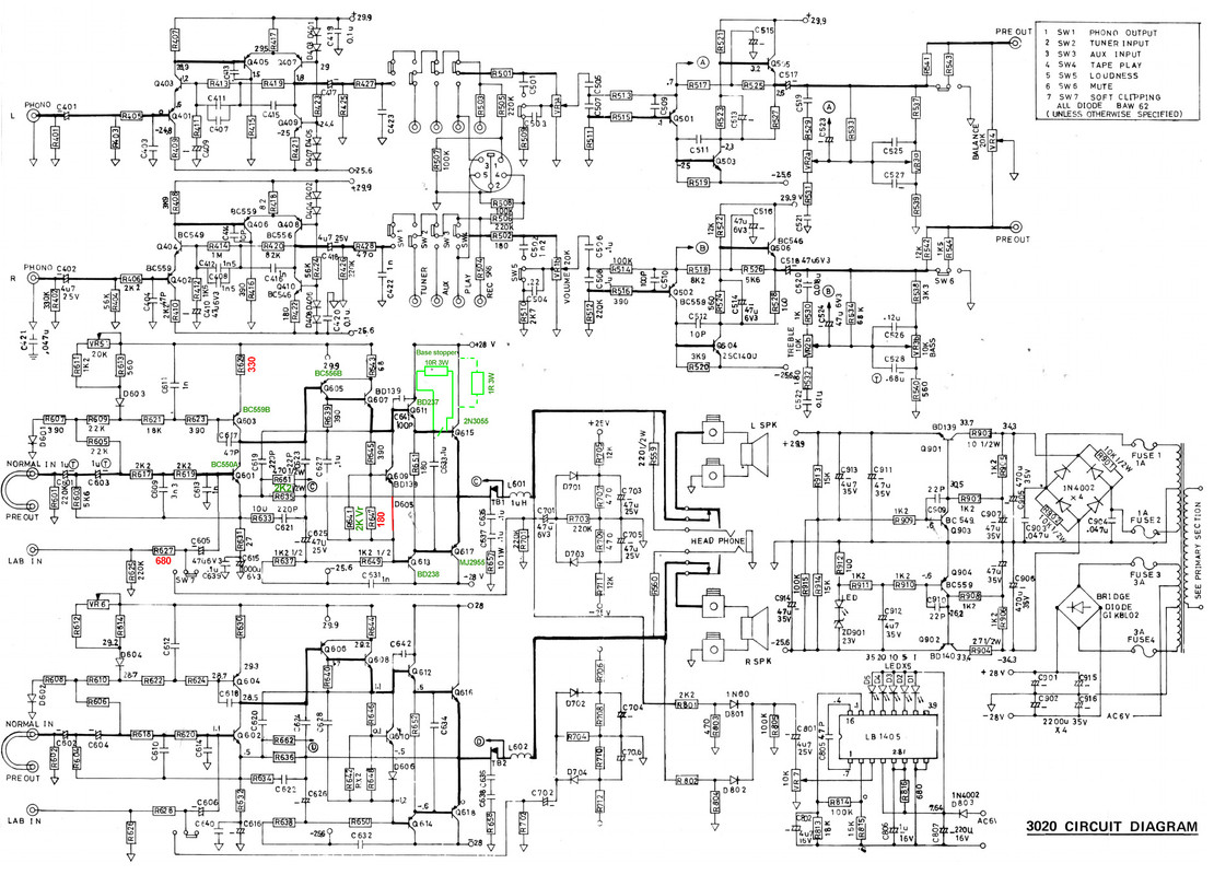
And there is the shematic after my modifications, All electrolytics have been changed for new ones (same value, higher voltage); the 6 tantals have been replaced with polyester film caps of the same value.
So to make things clear about my amp, here is the official schematic:
Then Here the amp I got before any modifications (seems like all differences are from manufacturer but I can't be sure (especially for the power bjts)
some resistors value have changed, a diode has been removed and replaced by a jumper wire and the 2n3055/MJ2955 have been replaced with BDW22C/24C
And there is the shematic after my modifications, All electrolytics have been changed for new ones (same value, higher voltage); the 6 tantals have been replaced with polyester film caps of the same value.
Last edited:
All right. You know my thoughts about this design and I agree that it seems a suicidial chap.
A few things I'm really concerned about and cannot follow the choises and solutions of the nad design team (no typo here!). It appears to me that this design was doomed in the first place but brought back to live with fingers crossed.
Why use 3055/2955 bjt's with 'build-in' degraded emitters? Cheaper?
Why use a current source load (Q603/604) on top on a collector output with only a Sziklai base as load, relying on a stable dc-feedback where pots VR5/6 are actually determining the behaviour of the current source which is in general not temperature stable. How to build a central heating oscillator...
Why this input 'ground-bootstrapping'.
Why the triple ac/dc/hf feedback on both sides of the 'safety-relay?
These are four 'ingenious inventions' with individual pro's and con's each, piling up to equal 'correction' mechanisms to keep the patient alive.
Now I've seen the phono stage too, I'm wavering between smart and stupid (RIAA feedback to cascode top bjt, false differential as output... boyoboy).
I would have fired this team.
The changes in the intermediate drawing are ok, save my previous remarks about dc setpoint changed by R635/636 and the related change of R629/630.
To prevent this circuit from going beserk at random, I would throw away this awkward current load Q603/604 to start with. Remove (left ch noted) Q603, R629, C617 and replace with a single 470 ohm resistor. That would be the corresponding value. Open loop gain will decrease considerable, but I guess the Sziklai (Q605-607) has enough gain on its own with the bootstrap load (R649-C625-R637). Now an unneeded stablility issue has been removed and the dc-loop can put its effort in stability of the amplifying circuit.
You did add emitterresistors (as rightly suggested by experienced others) to the BDW22C/24C couple? I would follow their advice without discussion.
The 'idle current measurement resistor' (1R3W) is needless now.
C615 and C625 are crucial so should have excellent specs. C603 and C605 are important too. In softclip mode, C605 can ruin the amp easely. Avoid this SC thing better. In the drawings, it appears that C603 is wrongly polarised, it should be as C604; positive pole on R605, neg on R603. Check dc value at nodes between C601-C603 / C602-C604 anyway and check position of caps is right.
Q's 609/610 must be mounted on the heatsink. If the omitted diode was put there, the bjt's have to take over.
That should be step number -1 at this point. If those still aren't in you don't have to be surprised if the thing goes into thermal runaway at random.You did add emitterresistors (as rightly suggested by experienced others) to the BDW22C/24C couple? I would follow their advice without discussion.
That's just how they were then, and seeing how more emitter resistance in Class (A)B amps increases distortion, you only want to add about as much as needed for thermal stability. It was cheaper, too.Why use 3055/2955 bjt's with 'build-in' degraded emitters? Cheaper?
That might be why you don't commonly see a current source load on singleton inputs.Why use a current source load (Q603/604) on top on a collector output with only a Sziklai base as load, relying on a stable dc-feedback where pots VR5/6 are actually determining the behaviour of the current source which is in general not temperature stable. How to build a central heating oscillator...
So they could have more RF filtering capacitance on the input?Why this input 'ground-bootstrapping'.
For some reason I think of the '3020 as a very British design, maybe because of its somewhat quirky, utilitarian nature. Someone familiar with UK conditions would also try to keep off longwave stations.... JLH certainly did.
Besides, the input transistor seems to be running a fair amount of current. Its base current would be responsible for a good amount of nonlinearity with a few kOhms running around there.
That's a fuse, I think. Not exactly the definition of pure canned linearity, hence why you want this inside the feedback loop if at all possible. You need an extra resistor to go in front of the fuse in case that ever blows, otherwise the output would latch up.Why the triple ac/dc/hf feedback on both sides of the 'safety-relay?
I think C619 (220p) is local negative feedback much like you might see on an opamp driving a discrete output stage... pole splitting and all. C623 is Miller compensation encompassing the output stage, not an approach for the faint of heart admittedly - as much as it keeps distortion down, stability can be a real issue.
Are you sure?To prevent this circuit from going beserk at random, I would throw away this awkward current load Q603/604 to start with. Remove (left ch noted) Q603, R629, C617 and replace with a single 470 ohm resistor. That would be the corresponding value.
Maybe 2 mA... 1.4something V... yeah, like a 680..750 or something. Still seems pretty low. Maybe that's why they had a current source there in the first place. Might need some level shifting action there if you want to get in a larger resistor (zener || C or LED || C or something).
All right. You know my thoughts about this design and I agree that it seems a suicidial chap.
A few things I'm really concerned about and cannot follow the choises and solutions of the nad design team (no typo here!). It appears to me that this design was doomed in the first place but brought back to live with fingers crossed.
Why use 3055/2955 bjt's with 'build-in' degraded emitters? Cheaper?
Why use a current source load (Q603/604) on top on a collector output with only a Sziklai base as load, relying on a stable dc-feedback where pots VR5/6 are actually determining the behaviour of the current source which is in general not temperature stable. How to build a central heating oscillator...
Why this input 'ground-bootstrapping'.
Why the triple ac/dc/hf feedback on both sides of the 'safety-relay?
These are four 'ingenious inventions' with individual pro's and con's each, piling up to equal 'correction' mechanisms to keep the patient alive.
Now I've seen the phono stage too, I'm wavering between smart and stupid (RIAA feedback to cascode top bjt, false differential as output... boyoboy).
I would have fired this team.
The changes in the intermediate drawing are ok, save my previous remarks about dc setpoint changed by R635/636 and the related change of R629/630.
To prevent this circuit from going beserk at random, I would throw away this awkward current load Q603/604 to start with. Remove (left ch noted) Q603, R629, C617 and replace with a single 470 ohm resistor. That would be the corresponding value. Open loop gain will decrease considerable, but I guess the Sziklai (Q605-607) has enough gain on its own with the bootstrap load (R649-C625-R637). Now an unneeded stablility issue has been removed and the dc-loop can put its effort in stability of the amplifying circuit.
You did add emitterresistors (as rightly suggested by experienced others) to the BDW22C/24C couple? I would follow their advice without discussion.
The 'idle current measurement resistor' (1R3W) is needless now.
C615 and C625 are crucial so should have excellent specs. C603 and C605 are important too. In softclip mode, C605 can ruin the amp easely. Avoid this SC thing better. In the drawings, it appears that C603 is wrongly polarised, it should be as C604; positive pole on R605, neg on R603. Check dc value at nodes between C601-C603 / C602-C604 anyway and check position of caps is right.
Q's 609/610 must be mounted on the heatsink. If the omitted diode was put there, the bjt's have to take over.
OK so I made pictures of your suggested modifications:
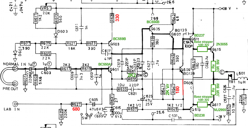
Here the addition of emitter resistors (0R33 5W as I got some of those on hand), I left the Base stoppers as they will not do any harm (as long as I can tell), I ain' t represented the Idle current measurement res as they are only needed during Bias adjustment.
And now the suppression of the current source load replaced by a 470R res
I'm not really sure about the placement of the 470R res, so please correct me if I'm wrong.
For the Sziklai it is best to have maximum control without anything in between, so connect top of the 470R (now on R623) close to top of R643, on the positive rail.
Forget about the rest of the cs circuit, it only provides base current for Q601 (harmless).
The 0.33/5W R's are ok. You might prefer less risk by substituting the 3055/2955 pair with cheaper BD139/140 combo and 10E emitter-resistors for testing purpose. The BD140 can easely swallow the current from Q601.
Turn R641 to max for minimum bias (390 + 2k//180 / 2k//180) * 0.6 = ~2V bias.
Do not turn R641 to zero, because this results in rail-to-rail bias. A stopper of 150E in series with R641 gives a max bias of 3.4V and must be sufficient.
If a current source as load for Q601 is needed, I'll post a screenshot of Sony's brilliant temp-stable fet-bjt compound as used in their Esprit series. Only a current mirror on top and you have your perfect cs.
Sony TA-E86B CurrentSource
R210 set the desired current, R209 is the pinch off of the fet devided by this current. R211 is a high value to keep Q206 at very low current (most current through R210). Zener D203 switches CS off when powering off.
Calculating R210 is 0.6V / desired current, use with a PNP-PNP currentmirror on top.
A very smart circuit.
I am a proud owner of this pre-amplifier for 35 years!
Attachments
Thanks a lot,
So If I understood everything well, here is the schematic with the test rig:
I'm not good enough to find the component values for the current source topology you posted, I 'll need help on this subjet if it happens to be necessary.
Q205 is a N-channel Fet right? and Q206 is supposed to be Q601 in the NAD schematic? So the whole topology replaces C611/Rr621/R623/R629/Q603 and C617, right?
Last edited:
- Home
- Amplifiers
- Solid State
- Early NAD 3020 fried channel