Have you considered bootstrapping from the emitters / sources already?
Maybe something similar like this just without CFPs:

Should fix the voltage across the transistors being cascoded without and issues related to phase lag. Not novel at all though.
Maybe something similar like this just without CFPs:
Should fix the voltage across the transistors being cascoded without and issues related to phase lag. Not novel at all though.
Thank you Lee.Have you considered bootstrapping from the emitters / sources already?
Maybe something similar like this just without CFPs:
View attachment 1084254
Should fix the voltage across the transistors being cascoded without and issues related to phase lag. Not novel at all though.
Will try it and report the results here.
Hi Lee
Do you have more information regarding the circuit you posted ?
I tryed to find it as I remenber having read about improved input stages but can not find any info.
The idea of biasing the two cascodes independently (keeping the differential action unchanged) seems to be very good indeed.
Kind regards
Ricardo
Hi Ricardo,
I have the concept from a paper Michael Kiwanuka wrote:
https://www.electronicsworld.co.uk/wp-content/uploads/2020/04/amps.pdf
You can see a simple implementation without CCS in figure 57, 59 and 60.
I just added CCS and replaced the diodes with LEDs.
I don't get why operating the transistors at near zero Vce should be any good, probably somebody else might know.
White or blue LEDs instead let the cascoded transistors operate at very low Vce and have low current noise, lower than Zeners at least.
Having independent cascodes for each transistor is especially useful if the voltage across both transistors is different.
In amplifier with a lot of GNFB, the differential voltage should be low as long as GNFB is high.
Thus the benefit is most notable once GNFB becomes less effective at higher frequencies or in amplifiers without GNFB.
Bootstrapping from the emitters should ensure the most constant Vce or Vds of the transistors and no phase shift.
Stealing current from those nodes is not without risk however.
The transistors Q5 and Q6 should have high hfe and low capacitance.
Base stoppers help to isolate the transistors capacitance from the emitter nodes.
Above snip of the schematic is taken from an amplifier I'm building right now.
I can't say yet whether this work well or not.
The previous revision had the cascode bases bootstrapped from the common emitter node of the LTP.
I plan a comparison of both options and I'm curious whether I can measure any difference.
Apart from inspiring you, I posted this to hopefully get some input from more experienced guys what they think about it.
Lee
Thank you very much for your contribution.
Now I understand why Michael used independent cascodes for each input transistor.
In my present design, following chip-mk suggestion, I am using Jfets instead of BJT to bootstrap the cascode bases to the input signal.
The high input impedance of the Jfets will reduce its interaction with the currents in the sources of the input jfets.
Also, in this case I am using a zener instead of a diode or led because I want the input Jfets to work with a minimum 10Vds.
Please see asc file below.
Attachments
I quickly did a simulation to figure out how much better the individual bootstrap from the emitter is than the scheme I used previously, which is just three LEDs in series between the tail node and the common bases of the cascodes.
Here is the situation with the differential cascodes:

That would be with bootstrapping from the tail:

All at 100kHz to exaggerate the effect. While my amplifier uses TPC, NFB is not very effective at such high frequency. Probably with plain Miller compensation, the effect would be more obvious.
Michael's scheme works better, but is it worth it? The more simple bootstrapping from the tail node works well, too.
Then I set up a voltage controlled voltage source with 4V voltage source on top to drive the cascodes from the VAS output:

Obviously the phase shift makes the non-inverting transistors Vce more variable.
The same driven from the amplifier output:

Not that much worse.
Just for fun I configured the cascodes reference to ground instead of any bootstrap:

Ouch, this is really bad!
I would conclude that bootstrapping is good overall, regardless if from the tail, the emitters, VAS or amplifier output. There are slightly better ways to do it and slightly worse.
I should have done such simulation much earlier.
Here is the situation with the differential cascodes:
That would be with bootstrapping from the tail:
All at 100kHz to exaggerate the effect. While my amplifier uses TPC, NFB is not very effective at such high frequency. Probably with plain Miller compensation, the effect would be more obvious.
Michael's scheme works better, but is it worth it? The more simple bootstrapping from the tail node works well, too.
Then I set up a voltage controlled voltage source with 4V voltage source on top to drive the cascodes from the VAS output:
Obviously the phase shift makes the non-inverting transistors Vce more variable.
The same driven from the amplifier output:
Not that much worse.
Just for fun I configured the cascodes reference to ground instead of any bootstrap:
Ouch, this is really bad!
I would conclude that bootstrapping is good overall, regardless if from the tail, the emitters, VAS or amplifier output. There are slightly better ways to do it and slightly worse.
I should have done such simulation much earlier.

Thank you Lee
I can confirm that all methods work well as I did try them in my protoboards.
Subjectively it seems that bootstrapping the bases of the cascodes to the IPS common emitter junction sounds slightly clear.
I can confirm that all methods work well as I did try them in my protoboards.
Subjectively it seems that bootstrapping the bases of the cascodes to the IPS common emitter junction sounds slightly clear.
Hi LK, may I know what is your rationale adding resistors R15, R16 in your circuit?Have you considered bootstrapping from the emitters / sources already?
Maybe something similar like this just without CFPs:
View attachment 1084254
I heard that those resistors may help with stability of the cascodes. Not sure.
Since I added base stoppers to the cascodes, R15 and R16 may be superfluous.
Since I added base stoppers to the cascodes, R15 and R16 may be superfluous.
Hi Lee
I have been studying your circuit and have some doubts:
Why did you use mid power bjt for the cascodes and the bootstrap followers q5..q8 ?
What type of ccs are you using for cascode biasing?
In the differential cascode like yours, the slightest current difference between the two ltp branches, might convert cm signals to dm, increasing distortion.
Both ccs must be matched... what type of ccs are you planning ?
Thank you very much for your input, this is exactly what I was looking for since the circuit is not used often and I don't have experience with it and don't know about possible pitfalls.
The reason for the mid power BJTs is that with a tail current of 8mA and a power supply voltage of up to 100V, dissipation is up to 0.4W in each cascode transistor. Small signal transistors typically don't come with SOA plots so I don't know whether this is still safe although within the typical dissipation limit for a TO-92 package transistor.
The SC3503 / SA1381 have very low capacitance and high speed.
For the bootstrap followers Q5 and Q6 I agree that low power and high voltage TO-92 transistors would not only do the job, but also perform even better. Maybe some SC1845 / SA992 or similar. I think about installing such transistors now - thanks.
I use cascoded LED referenced CCS for the cascode bias - nothing special.
Note that the LTP (innermost two connections on top) is loaded by active loads (see Bob Cordell's MOSFET amplifier with error correction for circuit details).
The bootstrap CCS (outermost two connections on top) are connected to the positive supply rail.
The risk that Q5 and Q6 are stealing current from the emitter of the LTP transistors causes imbalance in the LTP is real.
Thus the transistors Q5 and Q6 should have highest hfe to minimize the loss. Also low capacitance transistors would be good in order to not add capacitive load here.
I don't understand why matching of the cascode CCS is that critical.
In case the CCS current is unequal, the CCS imbalance would be rather small to begin with and be divided by the hfe of the bootstrap transistors Q5 and Q6.
I would try another option:
Use only one ccs feeding two large resistors connected to the bases of the cascodes... if the resistors are matched (ex: 10kohm) there should be no base current differences.
Also, as each ltp branch has its own cascode, there will be a base current cancellation in each side.... due to this base current cancellation you can connect the biasing leds directly to the ltp sources, without the followers q5 q6.
Also a small bypass cap over each led will help reduce ltp vce variations.
Simulation indicates even lower thd20 with this arrangement...
Let me know what you think..
Here I sketched what I understood you explained:

I agree that base current cancellation works and also that this seems to perform as good as the individual cascodes driven by the emitter followers.
CMRR seems to be as good as the other options.
The only thing that feels somewhat awkward is that the current from the cascode CCS is opposing the tail current through the emitter degeneration resistors. More a feeling than an engineering judgement. Any imbalance would show as DM, not CM. How about (10k) resistors tolerance?
Yes, any imbalance in the DM cascode bias currents will create an offset. CM signals will then be converted in DM and be amplifyed.
The only benefits I see in the DM cascode bias arrangement is that in this case, CM and DM signals in the cascode bases are bootstraped and so IPS bjt Vce are held constant for both types of signals and due to base current cancelation we can use a faster circuit without resorting to buffers.
In the case we use a CM cascode bias referenced to the IPS lower CCS (between the emitter resistors junction), any cascode bias current error will be CM and not amplified.... but in this case, cascode bias current impact should be minimized using a buffer.
My simulations indicate that in my VFB high open loop gain, high NFB design, the difference between the input and NFB signals in the LTP is minimal so a CM cascode bias circuit works perfectly.

PS:
I would use RED leds instead of Blue due to their much lower noise even at very low bias currents.
Ricardo
The only benefits I see in the DM cascode bias arrangement is that in this case, CM and DM signals in the cascode bases are bootstraped and so IPS bjt Vce are held constant for both types of signals and due to base current cancelation we can use a faster circuit without resorting to buffers.
In the case we use a CM cascode bias referenced to the IPS lower CCS (between the emitter resistors junction), any cascode bias current error will be CM and not amplified.... but in this case, cascode bias current impact should be minimized using a buffer.
My simulations indicate that in my VFB high open loop gain, high NFB design, the difference between the input and NFB signals in the LTP is minimal so a CM cascode bias circuit works perfectly.
PS:
I would use RED leds instead of Blue due to their much lower noise even at very low bias currents.
Ricardo
I10 in your circuit is way too high.... try using only 0,5mAHere I sketched what I understood you explained:
View attachment 1087698
I agree that base current cancellation works and also that this seems to perform as good as the individual cascodes driven by the emitter followers.
CMRR seems to be as good as the other options.
The only thing that feels somewhat awkward is that the current from the cascode CCS is opposing the tail current through the emitter degeneration resistors. More a feeling than an engineering judgement. Any imbalance would show as DM, not CM. How about (10k) resistors tolerance?
Also try different leds... 2xred maybe
Why is the current too high?
Red LEDs are less noisy than blue or white. I just can’t fit two in series on my PCB, that’s why.
Regarding noise generated by Zeners and LEDs there is an interesting discussion:
https://www.diyaudio.com/community/threads/some-noise-measurements-for-leds-and-zener-diodes.35821/
Red LEDs are less noisy than blue or white. I just can’t fit two in series on my PCB, that’s why.
Regarding noise generated by Zeners and LEDs there is an interesting discussion:
https://www.diyaudio.com/community/threads/some-noise-measurements-for-leds-and-zener-diodes.35821/
Using a fet for ccs, it can have higher output impedance running at lower currents.
Also we must minimize base bias current injected in the input sources/emitters.
Anyway I found better thd20 with lower bias current.
Also we must minimize base bias current injected in the input sources/emitters.
Anyway I found better thd20 with lower bias current.
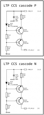
Here is a short follow-up:
I promised to write about any difference in performance of the two bootstrapping schemes I built.
However I blew up the front end module with the emitter buffered bootstrapping scheme so there are no results yet.
But I can report about practical CCS variation.
The schematic of my CCS is attached (you asked for the schematic earlier).
I measured 225mV across each 100R sense resistor (test points CP1 to CP2 and CN1 to CN2 in the schematic I posted previously).
While the current is slightly off compared to simulation (closer to 2mA), the two CCS show good matching with random parts from the same batch. So as long as the two CCS stay at the same temperature, the current output is very similar.
Attachments
- Home
- Amplifiers
- Solid State
- Driven Cascode Novelty Circuit