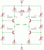
I'm a total newbie at such things, but I thought this would make a fine I/V converter for my new DAC. The DAC output is fed into a virtual ground between T1 and T2, trimmed to 0.0V. The current source T1 draws 10mA and V+ and V- sit at 6.75V steady state. The DAC output swings +/- 1.2mA giving a voltage swing of 2Vpp at the voltage terminal. R11 is the volume control.
The voltage swing could be brought up to 4Vpp by doubling R1/R6 and using a 5mA steady state current.
A few weeks ago I thought I might like to try the I/V stage from the Pass D-1, but it has too many parts (and MOSFETs) for my liking. I believe this design retains the advantages of the D-1 design without the overkill IRF610 MOSFETs.
Please post your scathing criticisms here. I already ordered the parts for it so I'll get to see it it works soon enough.
Attachments
I would bias the current sources a different way and use decent transistors. What is the 50 K resistor for? Ignore the guy from Pittsburgh. [joke]
Jocko
Jocko
I searched Google for "decent transistor" and didn't come up with anything. Maybe you can suggest something with the lofty specs of Ic > .0112mA and Vce > 10V? I just picked a decent one from a 2Nxxxx spec table.
How about something like Zetex 869? Geez $67 for 100! Okay okay, it's a lot less than the 4xPCM1704U-K 🙂
As for biasing I could bias with diodes or what-have-you but I calculate the current source should be within %0.1 with 1% resistors. What's the advantage?
How about something like Zetex 869? Geez $67 for 100! Okay okay, it's a lot less than the 4xPCM1704U-K 🙂
As for biasing I could bias with diodes or what-have-you but I calculate the current source should be within %0.1 with 1% resistors. What's the advantage?
LEDs make good references. Cheap and quiet.
Yeah, Harry would be proud that you looked on Google. He did a list somewhere on this forum. Do a search for "new law" (one of my more notorius threads) with HarryHaller. It is there somewhere. Stop using that simulator and just build it. It will work.
Those '1704s are getting pricey. The ungraded ones aren't that hot.
Jocko
What are you kidding? Simulate?! Do they even make those for Linux? I'm just glad I finally found something for drawing schematics.
Of course, it was the limitations of this "evaluation software" that inspired me to implement the entire digital receiver + dac section on a 3"x4" PCB!
Anyway the I/V is getting breadboarded first so I'll try resistors and LEDs and see what I like.
Thanks for the comments folks, I was fully expecting something along the lines of "That won't work because of X, fool."
Its not a attenuator. It is a regular resistor. The pin two of R11 is unused.The 50K R11 is the attenuator.
Don't pick nits. I used the symbol b/c its in the library. The attenuator isn't a pot, it's a stepped attenuator with 24 positions, where V+ is connected to GND and V- is connected to OUT. Sound backwards? Think it over for a while.
[ time passes ]
I only need two terminals of the attenuator because it works backwards in this circuit compared to a normal attenuator circuit. With the switch all the way up, I want the maximum resistance, and with the switch all the way down I want zero resistance.
[ time passes ]
I only need two terminals of the attenuator because it works backwards in this circuit compared to a normal attenuator circuit. With the switch all the way up, I want the maximum resistance, and with the switch all the way down I want zero resistance.
Jocko Homo said:Ignore the guy from Pittsburgh. [joke]
Jocko
😛
I've been doing some work on my own variation on the D1 theme if anyone is interested. Nothing special, but closer to normal supply voltages.
link
If the part count seems high, consider that the capacitors are really optional (but a very good idea).
Attachments
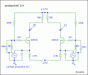
The DAC wants to see a virtual ground, and at zero volts. How are you ensuring the latter?
Jocko
Jocko
The design is for a DAC with virtual ground between 0v and AVdd. You could use it on a DAC like the 1704 by making the circuit's "virtual" ground the real ground and adjusting the trimming resistors appropriately.
The diagram is confusing...here is an update:
The diagram is confusing...here is an update:
Attachments
Not quite the way I would have done it. Remember I don't like MOSFETs, especially there. Should work though. Try to get the Z as low as possible. Yes, I know it will work if it is >0, but the lower the better.
(Hint: try a BJT.)
Jocko
(Hint: try a BJT.)
Jocko
Mosfet
Or you could put some feedback around mosfets gate to source to lower the impedance seen by the DAC. Or you could use inferior sounding BJTs.
H.H.
Or you could put some feedback around mosfets gate to source to lower the impedance seen by the DAC. Or you could use inferior sounding BJTs.
H.H.
- Status
- Not open for further replies.
- Home
- Source & Line
- Digital Source
- Drawing of I/V converter