Jacco how would you do that?
Jan
here is the explanation and a tutorial (4 minutes ):
https://www.youtube.com/watch?v=aYJQMZNfzIg
Duh, the reality is not like in the tutorial, elektor's pdf cannot directly be converted to gerber....
If someone can kindly do it, it would be great 🙂
have a nice day Jacco 🙂
If someone can kindly do it, it would be great 🙂
have a nice day Jacco 🙂
Duh, the reality is not like in the tutorial, elektor's pdf cannot directly be converted to gerber....
If someone can kindly do it, it would be great 🙂
have a nice day Jacco 🙂
Why not Eric? Seems straight-forward,the info is all there in the PDF.
Jan
Why not Eric? Seems straight-forward,the info is all there in the PDF.
Jan
Precisely, on the same page of the pdf there is the mirrored and the non mirrored version, it looks like the converter expects a single pcb picture per page...
If you can do it go ahead 😀 and share it , it would be very nice

Alternate route would be to convert the pdf images to bmp, import into the layout software, scale to size (pick a layer), rework and store in gerber format.
A pdf with multiple images can be split into individual image pdf's.
(adding the 2nd side of a board shouldn't be a lot of work if you have one side)
A pdf with multiple images can be split into individual image pdf's.
(adding the 2nd side of a board shouldn't be a lot of work if you have one side)
Last edited:
Precisely, on the same page of the pdf there is the mirrored and the non mirrored version, it looks like the converter expects a single pcb picture per page...
If you can do it go ahead 😀 and share it , it would be very nice
Very often a PDF also is build up in layers, don't know if that works. And sometimes Elektor publishes both top and bottom layer prints.
Worth a try sometimes.
Jan
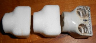
As a side note, modelling with digital cam images for 3D printing works like a charm by now.
Replacement mounting blocks for a shower door, lost one of the originals.
Also a better plastic, besides clean new ones on both sides.
Drilling the holes manually is more accurate, plus faster than adding them to the model.
(isn't this day and age fan-f-tastic )
)
Replacement mounting blocks for a shower door, lost one of the originals.
Also a better plastic, besides clean new ones on both sides.
Drilling the holes manually is more accurate, plus faster than adding them to the model.
(isn't this day and age fan-f-tastic
)Attachments
As a side note, modelling with digital cam images for 3D printing works like a charm by now.
Replacement mounting blocks for a shower door, lost one of the originals.
Also a better plastic, besides clean new ones on both sides.
Drilling the holes manually is more accurate, plus faster than adding them to the model.
(isn't this day and age fan-f-tastic
How much did it costed?
5-10 cents each (+ €5k for the dual extruder printer)
Just an example. The 3D software often manages to make a decent model by itself with a little over a dozen camera images.
In my years at university it was fun to do a 2D animated simulation in Excel. Not something you'd read in an Excel tutorial (MS graphics was running on Excel).
With pcb software it's also trial and error, what works depends on which package used.
5-10 cents each (+ €5k for the dual extruder printer)
Just an example. The 3D software often manages to make a decent model by itself with a little over a dozen camera images.
In my years at university it was fun to do a 2D animated simulation in Excel. Not something you'd read in an Excel tutorial (MS graphics was running on Excel).
With pcb software it's also trial and error, what works depends on which package used.
Very interesting. My first area of expertise was color reconstruction. It can be seen also as a higher dimensional reconstruction. But in thos years I was using Matlab 🙂
Do you own the extruder printer?😎
Yes, but I'm not in any way in the 3D printing business.
Bought as a test bed, to find out if one (possibly two) specific item can be made with 3D printing. With sufficient strength, accuracy, with which filament.
The things it usually prints take at least 16 hours, quite (too) often lasts into late night hours.
Printing the items I posted a picture of is educational, plus handy, saves searching for original manufacture ones.
(Buying one that laser-prints metal is next on the list, once those become available at a price level that doesn't buy a zero mileage convertible.
Printing pcb's would also be nice, as a bonus)
Last edited:
I try to upload an .rar file but a message appears "invalid file" the file is valid...why is this happening?
Yes, but I'm not in any way in the 3D printing business.
Bought as a test bed, to find out if one (possibly two) specific item can be made with 3D printing. With sufficient strength, accuracy, with which filament.
The things it usually prints take at least 16 hours, quite (too) often lasts into late night hours.
Printing the items I posted a picture of is educational, plus handy, saves searching for original manufacture ones.
(Buying one that laser-prints metal is next on the list, once those become available at a price level that doesn't buy a zero mileage convertible.
Printing pcb's would also be nice, as a bonus)
yessss!!!! printing multi-layers pcb would be great!!!!
Next step: a semi-conductor printer, so you can print transistors and even IC's 🙂
I try to upload an .rar file but a message appears "invalid file" the file is valid...why is this happening?
Because the forum software isn't set up to accept them. Put it in a zipped folder as long as its within file size limits and it should attach.
(.rars are not natively supported on a lot of PC's. Much better if its converted to pdf)
Because the forum software isn't set up to accept them. Put it in a zipped folder as long as its within file size limits and it should attach.
(.rars are not natively supported on a lot of PC's. Much better if its converted to pdf)
I wanted to include a fritzing PCB file that still needs a little work and improvements are welcome. 15 tl074 on a 10x10 cm should be very nice.
Critics are useless unless they come with an improved pcb 😀
File is attached as a .zip.
best regards
Attachments
I cant edit my previous post in order to delete the zip file that contains the PCB. It is obsolete, I have now a 18xTL074 much improved version.
How can I edit my own comments?
How can I edit my own comments?
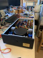
My 5532 Opamplifier build
Bought the boards from Elector some time ago. Originally had 2 power supply boards but that caused an insoluable (to me) ground loop. Chassis from eBay.
I like the sound. I seem to hear details that I hadn't noticed before. No A/B test though.
Regards,
Paul
Bought the boards from Elector some time ago. Originally had 2 power supply boards but that caused an insoluable (to me) ground loop. Chassis from eBay.
I like the sound. I seem to hear details that I hadn't noticed before. No A/B test though.
Regards,
Paul
Attachments
LF353 is one of the best ever made, interchanged with OPA2604 it's very hard to tell the difference. 2604 is a little quieter
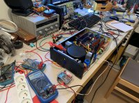
My NE5532 Bridge mode project build
Hy all,
I find this topic when I was in a NE5532 project myself and well, I finish it know and after all hours (days…) I pass on, I think it’ll be nice to share and show what’s going one.
I first see this design when reading D. Self “Audio power amplifier design” I find it very simple and interesting and decide to build my version of it with some “upgrade”.
My approach was :
1- Built bridge version (I have 6 ohms speakers… and more comfortable with 60W than 16W…)
2- Use the best quality component for each part I can pay for (Cost no object approach, regard to my limited budget..) for the best noise / linearity tradeoff.
3- Make it with SMD component as much as possible (for PCB area an noise consideration)
4- Exit the balanced input (XLR connector) and keep only the unbalanced one (RCA connector) because first, he is noisier, and second I don’t have XLR output on my preamp.
5- Built it on a case that feet my HiFi furniture (case home made with steel and aluminum scrap)
6- Make a symmetrical casing, because… I like it ! I think it look nice and make me feel like everything is in order, and track and cable length are match between each channel if ever that change something (for me optimizing the star grounding scheme at least)
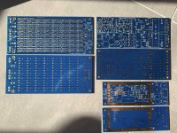
My implementation of the design was split into 12 boards (!) to fit these requirements as follow :
Power supply
1- Rectification board (Fuses, 220V filter, Bridge rectifier) x1
2- Filter board (2 Condos + 1 Self) x2 for +18V and -18V
3- Regulation board x2 for +18V and -18V
Signal
4- Input Preamp signal board x2 Left and right
5- Power board x4 (Bridge version so 2 for Left and 2 for Right)
Monitoring and protection
6- Ctrl board (Softstart, Faststop, diode+filter+DC speaker protection, LLLL saturation detection)
Power Supply (PCB 1, 2 and 3)
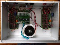
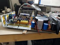
Nothing to say about power supply schema, It’s the original’s Self design. I just scale up everything for more current as my bridge version need and cut it into few PCB. Regulation is performed with LT1083 (7,5A max output current). Alimentation have the front half of the case on picture with +18V rail on left (red cable) and -18V rail on right (yellow cable). Ground at center point in the middle (start of black cable). Of course big toroidal transformer in the center of all these PCB, under the black steel shield.
Board 4 - Input Preamp signal PCB
I have to say, I pass few week-end and evening on this one ! I take the original design and try to optimize it from two way :
1 – Which AOP do I have to choose for each stage ? (5 stages (6 AOP) on Self’s preamp Design)
2 – Can I improve it by the use of parallel AOP technique here too ?
So I go very deep on AOP Datasheet for the “best in class” in audio use, and here are the shortlist I comeback from :
NE5532 : as reference and because it’s the original design choice. THD 0,002% (-95dB) (2 AOP per package)
NE5534A : Better voltage and current noise, and well match Vn/In. THD 0,002% (-95dB) (1 AOP per package)
LM4562 : For very nice noise specs and THD 0,00003% (-130,5dB) Better linearity in order of 66 compare with NE5532 ! (Best in class 2 AOP per package)
LME49990 : Best in class voltage noise and best in class linearity THD = 0,00001% (-140dB) = 0,1ppm distortion ! (1 AOP per package)
OPA627 : FET input AOP(all the other are BJT input), best in class for current noise THD = 0,00003 (-130,5dB)
AD797 : Almost as good as LME49990 for noise, and THD=0,0001 (-120 dB) (1 AOP per package)
So here are challengers. I didn’t put in the list AOP with input current cancelation circuitry as their specs are usually noisier.
LME49990 are obsolete and replace by OPA1611 by TI. I didn’t put it in the list because, first, the new one is not as good and I have LME49990 in stock so.
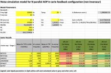
With this short list I went very deep in schema noise calculation for different AOP choice and configuration and I make a spreadsheet to calculate and compare option per stage. Some result for the first stage of that in Excel picture attached.
Here some ressources I use for building my noise model spreadsheet :
- Opamp noise calculator
- http://www.ti.com/lit/gpn/opa1656 (Page 18)
- https://www.analog.com/media/en/reference-design-documentation/design-notes/dn015f.pdf
- Book : “Operational Amplifier Noise: Techniques and Tips for Analyzing and Reducing Noise”
SEE ATTACHE SPREADSHEET SCREEN SHOT
Conclusion : for the first stage who use 2 parallel serie feedback AOP in original design. The best one is AD797, but it is not unity gain stable, and usually advise for bigger gain than only 3,41 in this stage. Datasheet advise matching input impedance too and we haven’t here so he didn’t suit well the need and I didn’t choose it. Second best choice (and first dual package choice) is LM4562 ! In fact it’s not the LME49990 because, the cost for his beautiful input voltage noise is the bigger Input current noise, and with the 47R source impedance, LM4562 is a better compromise between current and voltage noise for this source impedance. In fact all AOP have an optimum number of parallel device for noise figure and it’s depend on source and input impedance. Optimum is when Rsource // Rin = Vn / In. Exemple, for one LME49990 Vn / In = 314 ohms so for Rin = 47 kohms, optimum Rsource must be 317 ohms. Be careful, optimum Rsource vary with number of AOP in parallel, because current and voltage noise add themselves in a root square law, make some spreadsheet guy’s !
As you see, FET input OPA are out of the game for small source impedance because the beautifully input noise current came with “bad” voltage noise so we didn’t have enough noise advantage with noise current in 47R source for the voltage noise price of FET AOP.
And so on for other stage and the preamp PCB. I end-up with a mix of LME49990 and LM4562 for all the stage of this board and decide to keep the same number of AOP as original design for cost ($) and PCB area regard to benefit. I just change little things on input filter, and add input impedance matching circuitry on last stage from original design to optimize DC offset (see design remarque below). I find theorical -100,03 dBu of noise at the end of the board, SNR 124,94 dB.
I use brand quality for all component (buy on Mouser), polystyrene caps when I can, else polypropylene and some electrolytic for PCB decoupling. All resistor are smd THIN film type. So sade they are missing in D. SELF resistor technology article ! But after some reading, I’m thinking they are good enough compare with true-hole metal-film tech if not better ?
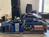
On picture, Preamp board are in the left and right corner of the case, nearest from input connector and as far as possible from supply and “HP big current” flowing. I made both side copper shield for the two board (Home made from a copper sheet, a little nightmare to build !)
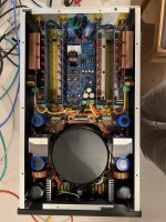
Board 5 – Power PCB
Very straight forward design, like original. Just a buch of follower of NE5532 with 1ohm current sharing resistor output. I use NE5532 instead of LM4562 for cost. (I buy 300 NE5532 for around 20€ in chineese website compare to 273€ for LM4562 on Mouser). Each of the 4 PCB have 56 of them. I want first to go to 64 for dual the original schema and have some room for driving 4ohms speaker, but I was out off PCB space and since my speaker are 6 ohms.
I calculate 56 is ok as they can delivered : 56 NE5532 per board so 112 AOP x38mA = 4,25A TYP and x60mA = 6,72A MAX.
Maximum peak to peak voltage swing is 26V so 9,19 Vrms into 3ohm give 3,06A. (3ohm because in bridge mode, we have two board per channel, running in opposing phase of each other, so they have to drive half of the load each and with 6 ohms speaker its 3 ohms per board) This give in theory 56W into 6 ohms. I measure 54W in practice before clipping.
112 parallel AOP will reduce the voltage noise by √112 = 10,58 (20,49 dB) and since the output noise of a 5532 voltage-follower is about – 119dBu, the noise from one power board alone will be –139,49 dBu (!). I don’t know if in bridge design (two board running out of phase) I can use the same formula for equivalent noise calculation including the two board, if yes for one channel (2 boards) it give √224 = 14,97 ( 23,5 dB) so 142,5 dBu. Somebody can tell me if it’s right please ?
I add big supply decoupling capacitor on each board compare to original design.
All signal board (6 of them) are put in vertical way in casing because it optimize the cooling with hot air moving from bottom to up the case. I made holes in casing up and down for that per power PCB.
Remarque : I read lots of post about using TL084 for this design in this topic. I have to say, even before tcheking output swing and current possibility, datasheets say voltage input noise 18 nV/√Hz, so 3,6 time more than NE5532 and THD = 0.003% so 1,5 more than NE5532. For a low noise and low distortion design, I think no need to go further ! and I even didn’t talk about all the other competitor in the room who are much more better for price consideration. After, it will work and I think not too bad, I agree with that
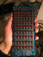
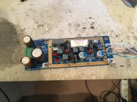
Board 6 – Control PCB
This control board is a mix off two design bloc.
Bloc 1 is speaker protection, I implement the softstart faststop who was in the supply board in original design. I just have to adapt it’s input to 4 PCB instead of 2. I put here too, relays, speaker diode protection, output RL filter. Self are upside down the PCB and at 90° angle to minimize induction crosstalk. All blue cable are output signal for speaker on photo.
Bloc 2 is LLLL for Log law level Led. It’s another D. Self-interesting design I find on small signal audio design book. And since it’s already a D. Self-design for amplifier part, I find funny to add another design from the same designer. The LLLL is just a circuitry who turn on and off a saturation LED per channel. They just use a quasi-log law to compare signal and reference, it make it more precise at the clipping point. I have to say, it work great, but it’s a lot of circuitry for making two LED blinking at clipping !
I make this board with metal film true hole resistor, since ctrl are not in the signal path, and thin film resistor are F… expensive !
All signal and ctrl PCB (all the blue one on picture) was design on 2 side PCB with ground plane both side. Just upper side of power PCB missing ground plane because it’s the first I made and didn’t know how to managing it on my software yet..
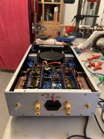
Casing
If front face I made only one button ON / OFF including blue power LED. (For instance, one button Hifi equipment have very good WAF ! )
And I had 3 LED, one light green when speaker connected (LSP ON), and two RED (one per channel) who blink when channel clipping.
Back face, 2 RCA input connector, 2 speaker output connector, one sector with fuse and one button who switch on and off the connection between circuitry ground and Earth chassis ground. I made that in all my Hifi conception, then I can play with for cut ground loop between hifi stuff if needed and then optimize total system hum.
Trouble I had during building
First my preamp board oscillate like hell ! I spend hour and hour to find why. I change all with NE5532 and its work, but not with LM4562 and LME49990. I find that it was because I add a small self in ground path for “isolate” HF between preamp ground and power ground in my design. I think it’s because high speed AOP are more sensitive to ground impedance, and so with self on it, they oscillate. However, I was thinking it was common practice. Is someone have something to say about it ?
Competition AOP need bigger decoupling caps as well as they are faster and I forget that so I add electrolytic caps in parallel of MKP for decoupling them and remove self on ground path and all run ok with first in class AOP I choose.
Relay control : I put 4 relay on my ctrl board. During start transition, they move very slow and oscillate a bit before stabilize. It work but I hate the startup sound ! So I had some capacitance on it, and I burn the controlling transistor… So I change the filtering for driving Relay and it work, but I’m still not very happy with. If I have to redo it, I’ll change, the relay ctrl and filtering on design and PCB.
DC fault control : I made mistake on my PCB, and few ground connection was erase when I do the labeling. Just have so make few solder adjustment on track.
For the rest, so far so good 🙂
Design notes
- I read lattely Self on Audio book, D. Self talking about adding a output resistor to V+ for add more linearization of output stage for the cost of current. Maybe I had implement that if I read earlier.
- In bridge mode, one of the two board in one channel are “outside” the DC servo loop (one for two board…) so one board have DC offset of the phase inverter AOP and power board. I find 2mV on my amp. As it’s very small and in bridge mode, speaker are “floating” from main ground, I can live with, but I think, design can be upgraded for include that in bridge mode.
Final conclusion
I start from a very simple design, but at the end so much work was done and I’m very happy with the result. My biggest frustration is that I didn’t have the equipment to measure THD, noise Etc, so I work in blind mode and cannot confirm my theorical work in practice and that is very frustrating. I dream of a Audio-Precision device !
For the sound, no precise measure I can do with my poor scope. I can just say, when ON and no music playing, my speaker are dead silent, even with my ear at 20cm far from the ribbon tweeter ! And the sound, clear, precise, far better than all I had at home (not so much..), so really happy with.
He was so quiet then now, my preamp dominate as hell the hum in my system, so I start to work on a new preamp as next project.. based on D. Self’s articles of course . My design “mix” Precision preamp and 2012 preamp article. Maybe a future article if they are a topic on it in this forum.
Thank’s if you read so far ! I hope this can help some of you to give a try to this very nice and comprehensive design, Regards Jean-Baptiste.
Hy all,
I find this topic when I was in a NE5532 project myself and well, I finish it know and after all hours (days…) I pass on, I think it’ll be nice to share and show what’s going one.
I first see this design when reading D. Self “Audio power amplifier design” I find it very simple and interesting and decide to build my version of it with some “upgrade”.
My approach was :
1- Built bridge version (I have 6 ohms speakers… and more comfortable with 60W than 16W…)
2- Use the best quality component for each part I can pay for (Cost no object approach, regard to my limited budget..) for the best noise / linearity tradeoff.
3- Make it with SMD component as much as possible (for PCB area an noise consideration)
4- Exit the balanced input (XLR connector) and keep only the unbalanced one (RCA connector) because first, he is noisier, and second I don’t have XLR output on my preamp.
5- Built it on a case that feet my HiFi furniture (case home made with steel and aluminum scrap)
6- Make a symmetrical casing, because… I like it ! I think it look nice and make me feel like everything is in order, and track and cable length are match between each channel if ever that change something (for me optimizing the star grounding scheme at least)
My implementation of the design was split into 12 boards (!) to fit these requirements as follow :
Power supply
1- Rectification board (Fuses, 220V filter, Bridge rectifier) x1
2- Filter board (2 Condos + 1 Self) x2 for +18V and -18V
3- Regulation board x2 for +18V and -18V
Signal
4- Input Preamp signal board x2 Left and right
5- Power board x4 (Bridge version so 2 for Left and 2 for Right)
Monitoring and protection
6- Ctrl board (Softstart, Faststop, diode+filter+DC speaker protection, LLLL saturation detection)
Power Supply (PCB 1, 2 and 3)
Nothing to say about power supply schema, It’s the original’s Self design. I just scale up everything for more current as my bridge version need and cut it into few PCB. Regulation is performed with LT1083 (7,5A max output current). Alimentation have the front half of the case on picture with +18V rail on left (red cable) and -18V rail on right (yellow cable). Ground at center point in the middle (start of black cable). Of course big toroidal transformer in the center of all these PCB, under the black steel shield.
Board 4 - Input Preamp signal PCB
I have to say, I pass few week-end and evening on this one ! I take the original design and try to optimize it from two way :
1 – Which AOP do I have to choose for each stage ? (5 stages (6 AOP) on Self’s preamp Design)
2 – Can I improve it by the use of parallel AOP technique here too ?
So I go very deep on AOP Datasheet for the “best in class” in audio use, and here are the shortlist I comeback from :
NE5532 : as reference and because it’s the original design choice. THD 0,002% (-95dB) (2 AOP per package)
NE5534A : Better voltage and current noise, and well match Vn/In. THD 0,002% (-95dB) (1 AOP per package)
LM4562 : For very nice noise specs and THD 0,00003% (-130,5dB) Better linearity in order of 66 compare with NE5532 ! (Best in class 2 AOP per package)
LME49990 : Best in class voltage noise and best in class linearity THD = 0,00001% (-140dB) = 0,1ppm distortion ! (1 AOP per package)
OPA627 : FET input AOP(all the other are BJT input), best in class for current noise THD = 0,00003 (-130,5dB)
AD797 : Almost as good as LME49990 for noise, and THD=0,0001 (-120 dB) (1 AOP per package)
So here are challengers. I didn’t put in the list AOP with input current cancelation circuitry as their specs are usually noisier.
LME49990 are obsolete and replace by OPA1611 by TI. I didn’t put it in the list because, first, the new one is not as good and I have LME49990 in stock so.
With this short list I went very deep in schema noise calculation for different AOP choice and configuration and I make a spreadsheet to calculate and compare option per stage. Some result for the first stage of that in Excel picture attached.
Here some ressources I use for building my noise model spreadsheet :
- Opamp noise calculator
- http://www.ti.com/lit/gpn/opa1656 (Page 18)
- https://www.analog.com/media/en/reference-design-documentation/design-notes/dn015f.pdf
- Book : “Operational Amplifier Noise: Techniques and Tips for Analyzing and Reducing Noise”
SEE ATTACHE SPREADSHEET SCREEN SHOT
Conclusion : for the first stage who use 2 parallel serie feedback AOP in original design. The best one is AD797, but it is not unity gain stable, and usually advise for bigger gain than only 3,41 in this stage. Datasheet advise matching input impedance too and we haven’t here so he didn’t suit well the need and I didn’t choose it. Second best choice (and first dual package choice) is LM4562 ! In fact it’s not the LME49990 because, the cost for his beautiful input voltage noise is the bigger Input current noise, and with the 47R source impedance, LM4562 is a better compromise between current and voltage noise for this source impedance. In fact all AOP have an optimum number of parallel device for noise figure and it’s depend on source and input impedance. Optimum is when Rsource // Rin = Vn / In. Exemple, for one LME49990 Vn / In = 314 ohms so for Rin = 47 kohms, optimum Rsource must be 317 ohms. Be careful, optimum Rsource vary with number of AOP in parallel, because current and voltage noise add themselves in a root square law, make some spreadsheet guy’s !
As you see, FET input OPA are out of the game for small source impedance because the beautifully input noise current came with “bad” voltage noise so we didn’t have enough noise advantage with noise current in 47R source for the voltage noise price of FET AOP.
And so on for other stage and the preamp PCB. I end-up with a mix of LME49990 and LM4562 for all the stage of this board and decide to keep the same number of AOP as original design for cost ($) and PCB area regard to benefit. I just change little things on input filter, and add input impedance matching circuitry on last stage from original design to optimize DC offset (see design remarque below). I find theorical -100,03 dBu of noise at the end of the board, SNR 124,94 dB.
I use brand quality for all component (buy on Mouser), polystyrene caps when I can, else polypropylene and some electrolytic for PCB decoupling. All resistor are smd THIN film type. So sade they are missing in D. SELF resistor technology article ! But after some reading, I’m thinking they are good enough compare with true-hole metal-film tech if not better ?
On picture, Preamp board are in the left and right corner of the case, nearest from input connector and as far as possible from supply and “HP big current” flowing. I made both side copper shield for the two board (Home made from a copper sheet, a little nightmare to build !)
Board 5 – Power PCB
Very straight forward design, like original. Just a buch of follower of NE5532 with 1ohm current sharing resistor output. I use NE5532 instead of LM4562 for cost. (I buy 300 NE5532 for around 20€ in chineese website compare to 273€ for LM4562 on Mouser). Each of the 4 PCB have 56 of them. I want first to go to 64 for dual the original schema and have some room for driving 4ohms speaker, but I was out off PCB space and since my speaker are 6 ohms.
I calculate 56 is ok as they can delivered : 56 NE5532 per board so 112 AOP x38mA = 4,25A TYP and x60mA = 6,72A MAX.
Maximum peak to peak voltage swing is 26V so 9,19 Vrms into 3ohm give 3,06A. (3ohm because in bridge mode, we have two board per channel, running in opposing phase of each other, so they have to drive half of the load each and with 6 ohms speaker its 3 ohms per board) This give in theory 56W into 6 ohms. I measure 54W in practice before clipping.
112 parallel AOP will reduce the voltage noise by √112 = 10,58 (20,49 dB) and since the output noise of a 5532 voltage-follower is about – 119dBu, the noise from one power board alone will be –139,49 dBu (!). I don’t know if in bridge design (two board running out of phase) I can use the same formula for equivalent noise calculation including the two board, if yes for one channel (2 boards) it give √224 = 14,97 ( 23,5 dB) so 142,5 dBu. Somebody can tell me if it’s right please ?
I add big supply decoupling capacitor on each board compare to original design.
All signal board (6 of them) are put in vertical way in casing because it optimize the cooling with hot air moving from bottom to up the case. I made holes in casing up and down for that per power PCB.
Remarque : I read lots of post about using TL084 for this design in this topic. I have to say, even before tcheking output swing and current possibility, datasheets say voltage input noise 18 nV/√Hz, so 3,6 time more than NE5532 and THD = 0.003% so 1,5 more than NE5532. For a low noise and low distortion design, I think no need to go further ! and I even didn’t talk about all the other competitor in the room who are much more better for price consideration. After, it will work and I think not too bad, I agree with that
Board 6 – Control PCB
This control board is a mix off two design bloc.
Bloc 1 is speaker protection, I implement the softstart faststop who was in the supply board in original design. I just have to adapt it’s input to 4 PCB instead of 2. I put here too, relays, speaker diode protection, output RL filter. Self are upside down the PCB and at 90° angle to minimize induction crosstalk. All blue cable are output signal for speaker on photo.
Bloc 2 is LLLL for Log law level Led. It’s another D. Self-interesting design I find on small signal audio design book. And since it’s already a D. Self-design for amplifier part, I find funny to add another design from the same designer. The LLLL is just a circuitry who turn on and off a saturation LED per channel. They just use a quasi-log law to compare signal and reference, it make it more precise at the clipping point. I have to say, it work great, but it’s a lot of circuitry for making two LED blinking at clipping !
I make this board with metal film true hole resistor, since ctrl are not in the signal path, and thin film resistor are F… expensive !
All signal and ctrl PCB (all the blue one on picture) was design on 2 side PCB with ground plane both side. Just upper side of power PCB missing ground plane because it’s the first I made and didn’t know how to managing it on my software yet..
Casing
If front face I made only one button ON / OFF including blue power LED. (For instance, one button Hifi equipment have very good WAF ! )
And I had 3 LED, one light green when speaker connected (LSP ON), and two RED (one per channel) who blink when channel clipping.
Back face, 2 RCA input connector, 2 speaker output connector, one sector with fuse and one button who switch on and off the connection between circuitry ground and Earth chassis ground. I made that in all my Hifi conception, then I can play with for cut ground loop between hifi stuff if needed and then optimize total system hum.
Trouble I had during building
First my preamp board oscillate like hell ! I spend hour and hour to find why. I change all with NE5532 and its work, but not with LM4562 and LME49990. I find that it was because I add a small self in ground path for “isolate” HF between preamp ground and power ground in my design. I think it’s because high speed AOP are more sensitive to ground impedance, and so with self on it, they oscillate. However, I was thinking it was common practice. Is someone have something to say about it ?
Competition AOP need bigger decoupling caps as well as they are faster and I forget that so I add electrolytic caps in parallel of MKP for decoupling them and remove self on ground path and all run ok with first in class AOP I choose.
Relay control : I put 4 relay on my ctrl board. During start transition, they move very slow and oscillate a bit before stabilize. It work but I hate the startup sound ! So I had some capacitance on it, and I burn the controlling transistor… So I change the filtering for driving Relay and it work, but I’m still not very happy with. If I have to redo it, I’ll change, the relay ctrl and filtering on design and PCB.
DC fault control : I made mistake on my PCB, and few ground connection was erase when I do the labeling. Just have so make few solder adjustment on track.
For the rest, so far so good 🙂
Design notes
- I read lattely Self on Audio book, D. Self talking about adding a output resistor to V+ for add more linearization of output stage for the cost of current. Maybe I had implement that if I read earlier.
- In bridge mode, one of the two board in one channel are “outside” the DC servo loop (one for two board…) so one board have DC offset of the phase inverter AOP and power board. I find 2mV on my amp. As it’s very small and in bridge mode, speaker are “floating” from main ground, I can live with, but I think, design can be upgraded for include that in bridge mode.
Final conclusion
I start from a very simple design, but at the end so much work was done and I’m very happy with the result. My biggest frustration is that I didn’t have the equipment to measure THD, noise Etc, so I work in blind mode and cannot confirm my theorical work in practice and that is very frustrating. I dream of a Audio-Precision device !
For the sound, no precise measure I can do with my poor scope. I can just say, when ON and no music playing, my speaker are dead silent, even with my ear at 20cm far from the ribbon tweeter ! And the sound, clear, precise, far better than all I had at home (not so much..), so really happy with.
He was so quiet then now, my preamp dominate as hell the hum in my system, so I start to work on a new preamp as next project.. based on D. Self’s articles of course . My design “mix” Precision preamp and 2012 preamp article. Maybe a future article if they are a topic on it in this forum.
Thank’s if you read so far ! I hope this can help some of you to give a try to this very nice and comprehensive design, Regards Jean-Baptiste.
Attachments
-
 Power PCB almost finish.jpg825.7 KB · Views: 496
 -
 PCB.jpg1.1 MB · Views: 457
 -
 Noise simulation Spreadsheet.png336.5 KB · Views: 430
 -
 CTRL PCB assembly.jpg981.6 KB · Views: 430
 -
 Case back finish.jpg685.7 KB · Views: 451
 -
 Amplifier top view final before closing case.jpg660 KB · Views: 601
 -
 Amplifier front view final before closing case.jpg484.7 KB · Views: 603
 -
 Amp under test with all front LED lighting.jpg909.2 KB · Views: 596
 -
 Amp side view.jpg787.3 KB · Views: 609
 -
 Premp PCB (without copper shield) decoupling eltrolitic caps add and ground self remove.jpg242.9 KB · Views: 501

- Home
- Amplifiers
- Chip Amps
- Doug Selfs NE5532 Power Amp. Thoughts anyone !