I think you are expecting to see a sine wave signal from output of power fets relative to mid point but you don’t bother to put an LC filter? If my suspicion is correct, then, hurry up!!! Put an LC filter right away before the adept guys appear to castigate you for this!!! LOL!😀.(Just kidding😛)
You have to google about the purpose of LC filter in class D. For the meantime, if LC filter is not yet available then you can use RC filter just for checking the output of the reference signal. It’s a good idea to put temporary 2 amp fast blow fuse to your Main DC supply. This will protect your circuit in case shoot through or accidental short circuit will occur. There are several hurdles that you will encounter along the way, so be prepared and make some research for your own enlightenment. Don’t forget, patience is a virtue.You’re almost there dude.
You have to google about the purpose of LC filter in class D. For the meantime, if LC filter is not yet available then you can use RC filter just for checking the output of the reference signal. It’s a good idea to put temporary 2 amp fast blow fuse to your Main DC supply. This will protect your circuit in case shoot through or accidental short circuit will occur. There are several hurdles that you will encounter along the way, so be prepared and make some research for your own enlightenment. Don’t forget, patience is a virtue.You’re almost there dude.
I think you are expecting to see a sine wave signal from output of power fets relative to mid point but you don’t bother to put an LC filter? If my suspicion is correct, then, hurry up!!! Put an LC filter right away before the adept guys appear to castigate you for this!!! LOL!😀.(Just kidding😛)
You have to google about the purpose of LC filter in class D. For the meantime, if LC filter is not yet available then you can use RC filter just for checking the output of the reference signal. It’s a good idea to put temporary 2 amp fast blow fuse to your Main DC supply. This will protect your circuit in case shoot through or accidental short circuit will occur. There are several hurdles that you will encounter along the way, so be prepared and make some research for your own enlightenment. Don’t forget, patience is a virtue.You’re almost there dude.
Oh boy it's been a while.. Well since my last post, i've followed on with your schematic and it worked fine. I got the amplifier to play through to the Loudspeaker. At the cost of adept guys having a go at me, yes i didn't use any LC filter, and just fed the 2 level modulation into the speakers directly.
Yes i do get shoot-through, so i'm in the process of adding a RCD network to set some dead time to avoid it.
I'm in the middle of removing the schmitt trigger you used and using LM361N comparators to split the signal into high and low. The propagation delay on these comparators is only 20ns compared to the schmitt trigger.
The split signals then go into my RCD network, before i use another LM361N comparator to act as a schmitt trigger to produce dead band adjusted PWM.
After that its literally just the rest of your circuit and I'll include the LC filter this time around.
I did something stupid and feeded too much current into the breadboard (second model) and i didn't know they can only handle up to 0.5A only.
So ever since then the PWM part has been acting wonky and it's been a pain because I have had to use another breadboard, new components and wires as well..And even after all that, there is a offset out of the collector output of the TL494 which i cannot explain. There's almost like a 1 volt offset which is weird because same wiring as in model 1 and i saw no offset.
Luckily I have saved the first working model separately and haven't fiddled around with it, so there is always that to fall back to everything else fails.
Can you explain me this or it might just be me. But when you don't connect the collector output to the schmitt trigger, why is the waveform i observe is always either a constant 12V pulled high by the resistor or 5V now that I'm working with TTL. Whereas it's normal PWM when the schmitt trigger is functioning.
Eva wrote:
Shouldn't the iput logic of the IR2110 be fed from a 5 V rail when the inputs are fed by the outputs of a 74HC... ?
Regards
Charles
Thanks for stating this. I'll pull Vdd to my 5V supply instead of 12V like before.
Oh the supplies I'm using have both voltage and current limiting. So i can limit the max current going through the MOSFETS.
Ledmania I have another question (Yes I know I'm full of questions).
In your schematic you adjust the pot to make sure the Duty Cycle is 50%, which means that the output voltage going to the speakers is basically half the supply.
So how are you doing gain adjustment in your amplifier?
You control the output voltage being fed into the speaker by adjusting the duty cycle of the Pulse Width entering the gate of MOSFETS.
So i thought that's where the Pot comes in and you can vary the voltage going into the input of the error amplifier in the TL494 between 1V to 3V (roughly) and you adjust duty cycle.
But in your own thread as well as here in mine. You've strongly stated adjusting the Pot to 50% Duty Cycle. If so how do you regulate the output voltage mate?
Oh also, I have symmetrical dead time of about 250ns on either side. I started with such high dead time on purpose just for the sake of testing. I will reduce it little by little until i get it right.
I still have that 1 volt offset which is annoying but this time around (Third model), both the Hin and Lin pulses are nice. Truly nice, no ringing effect at all. Unlike the last time i observed and saw crazy ringing because of the cross-over.
Can you explain me this or it might just be me. But when you don't connect the collector output to the schmitt trigger, why is the waveform i observe is always either a constant 12V pulled high by the resistor or 5V now that I'm working with TTL. Whereas it's normal PWM when the schmitt trigger is functioning.
I don’t understand this question but I will try.
Most probably you are measuring it with scope, so normally you’ll see 12v component signal out of you PWM. Try to measure it with DMM and you’ll see that PWM @ 50% will read as 6v. Same is true with your TTL at 5v will read 2.5v @ 50% duty..
Ledmania I have another question (Yes I know I'm full of questions).
In your schematic you adjust the pot to make sure the Duty Cycle is 50%, which means that the output voltage going to the speakers is basically half the supply.
Yes, half the supply referenced to global gnd but 0v across the speaker ref to mid point.
how are you doing gain adjustment in your amplifier?
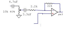
Those opamps behaves exactly as standard opamps which obey in a conventional opamp gain equation of: 22k/2.2k=10. So, the input sensitivity is 150mv giving an output of 1.5V @ pin 3. This way you can vary their gain by the ratio of those R.
Note; do not exceed more than 1.5V @ pin 3.
you control the output voltage being fed into the speaker by adjusting the duty cycle of the Pulse Width entering the gate of MOSFETS.
Yes. But this pot is for “DC” bias for centering the output duty to 50% only.
i thought that's where the Pot comes in and you can vary the voltage going into the input of the error amplifier in the TL494 between 1V to 3V (roughly) and you adjust duty cycle.
No. Once that pot was calibrated to 2v as the Vref @ pin 15, no further adjustment is necessary. Simply, 2v @ pin 16= 2v @ pin 3= 50% duty @ output of power fets.
but in your own thread as well as here in mine. You've strongly stated adjusting the Pot to 50% Duty Cycle. If so how do you regulate the output voltage mate?
You don’t have to regulate the output voltage but instead, 50% duty cycle is the required resting position @ the output of power fets “without audio” then this 50% is being modulated by +/_ 50% of your audio input @ full volume or +/_ less % @ low volume.. (tl494 cant go more than +/_50% but less than that)
Most of your questions can be observed through your actual circuits on hand with the aid of your scope. You have to explore your circuit by poking the scope’s probes to nodes of interest, pin 16, 15, 3. to pin 11/8, output fet, pre or post filter and across speaker. Just modulate the input and check the
output.
Cheers
ledmania
When I’m reading my post above, I think I’m giving more confusion to you😀.
I mean you don’t have to regulate the voltage across the speaker because this should be always 0v relative to mid point (50% duty no audio) and you’ll get AC signal when there’s audio present.
I mean you don’t have to regulate the voltage across the speaker because this should be always 0v relative to mid point (50% duty no audio) and you’ll get AC signal when there’s audio present.
Your project is getting more expensive by adding LM361N. This will negate the concept of being cheap class D. I think you will consume four LM361N?.
My old schematic shows I use Schmitt inverter but it is more suitable to use CMOS inverter like 74C04 as the phase splitter as well.
I’ve done simulations with this and it worked fine in providing adjustable deadtime.
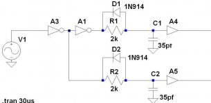
The 2 caps c1 and c2 are not discrete part of the circuit but it is the capacitive input of IR fet driver. A4 and A5 is the input buffer of fet driver. V1 gen is the output of tl494. this is better than RD at the gate of power fets and cheaper than LM316 approach.
My old schematic shows I use Schmitt inverter but it is more suitable to use CMOS inverter like 74C04 as the phase splitter as well.
I’ve done simulations with this and it worked fine in providing adjustable deadtime.
The 2 caps c1 and c2 are not discrete part of the circuit but it is the capacitive input of IR fet driver. A4 and A5 is the input buffer of fet driver. V1 gen is the output of tl494. this is better than RD at the gate of power fets and cheaper than LM316 approach.
Attachments
Last edited:
Those opamps behaves exactly as standard opamps which obey in a conventional opamp gain equation of: 22k/2.2k=10. So, the input sensitivity is 150mv giving an output of 1.5V @ pin 3. This way you can vary their gain by the ratio of those R.
Note; do not exceed more than 1.5V @ pin 3.
And the minimum voltage across pin 3 I should never go below? Because if that's the case I'll just add a variable resistor going upto 22K only, giving me a gain of upto 10.
No. Once that pot was calibrated to 2v as the Vref @ pin 15, no further adjustment is necessary. Simply, 2v @ pin 16= 2v @ pin 3= 50% duty @ output of power fets.
Right, upto to 50% duty cycle like you said. So can go below 50% duty cycle but not above. So i get max volume at 50% Duty Cycle and minimum volume at lower duty cycle.
Most of your questions can be observed through your actual circuits on hand with the aid of your scope. You have to explore your circuit by poking the scope’s probes to nodes of interest, pin 16, 15, 3. to pin 11/8, output fet, pre or post filter and across speaker. Just modulate the input and check the
output.
Allright thanks. I wanted to perform gain adjustment so that i can control the volume of the sound. I'll observe pin's 16,15, 3 and pins 8 and 11 for the TL494.
Your project is getting more expensive by adding LM361N. This will negate the concept of being cheap class D. I think you will consume four LM361N?.
My old schematic shows I use Schmitt inverter but it is more suitable to use CMOS inverter like 74C04 as the phase splitter as well.
I’ve done simulations with this and it worked fine in providing adjustable deadtime.
The 2 caps c1 and c2 are not discrete part of the circuit but it is the capacitive input of IR fet driver. A4 and A5 is the input buffer of fet driver. V1 gen is the output of tl494. this is better than RD at the gate of power fets and cheaper than LM316 approach.
I use three LM361N. The A3 and A1 blocks in your diagram, a single LM361N gives me that with propagation delay of maximum 20ns. I have exactly the same RCD network as in that diagram and A4 and A5 are my other two LM361N.
Sorry I hope I'm being clear and not confusing you. I'd like to control volume of the speaker and i can do this by adjusting the gain of the error amplifier through the resistors 22k/2.2K = 10 ?
So using a variable resistor (Trimpot) i can reduce the 22k down to whatever and i reduce gain, so I reduce volume as well?
Everything else in the TL494 connection i leave untouched, just the 22k resistor i change?
And I make sure that the voltage from pin 3 never exceeds 1.5V.
So using a variable resistor (Trimpot) i can reduce the 22k down to whatever and i reduce gain, so I reduce volume as well?
Everything else in the TL494 connection i leave untouched, just the 22k resistor i change?
And I make sure that the voltage from pin 3 never exceeds 1.5V.
Sorry I hope I'm being clear and not confusing you. I'd like to control volume of the speaker and i can do this by adjusting the gain of the error amplifier through the resistors 22k/2.2K = 10 ?
So using a variable resistor (Trimpot) i can reduce the 22k down to whatever and i reduce gain, so I reduce volume as well?
Everything else in the TL494 connection i leave untouched, just the 22k resistor i change?
And I make sure that the voltage from pin 3 never exceeds 1.5V.
If you want to put a volume control, then it is not good to alter the gain of the opamp with that 22k resistor. This will jeopardize the output of pin 3 when the volume is in minimum resistance.
Just simply put at least 4.7uf cap in series with 10k pot parallel to your audio source relative to ground then the center of that pot goes to coupling cap @ the input of opamp and that’s it. Your done.
In an open loop design volume control may be achieved by changing gain, but in closed loop amplifiers many properties are dependent on gain, including frequency response, so a voltage divider (potentiometer) before the amp has to be used instead.
If you want to put a volume control, then it is not good to alter the gain of the opamp with that 22k resistor. This will jeopardize the output of pin 3 when the volume is in minimum resistance.
Just simply put at least 4.7uf cap in series with 10k pot parallel to your audio source relative to ground then the center of that pot goes to coupling cap @ the input of opamp and that’s it. Your done.
Ok putting the capacitor in series with the Pot I understand. But I lose you when you say "parallel to your audio source relative to ground".
Do you mean like so ?
http://img7.imageshack.us/i/volumem.png/
Hi Guys,
I need to build a triangular wave generator which is absolutely linear (or atleast as far as possible) hence I thought of looking at this forum for some useful tips. Does anyone know of a schematic for this ?
Cheers,
Trevor
I need to build a triangular wave generator which is absolutely linear (or atleast as far as possible) hence I thought of looking at this forum for some useful tips. Does anyone know of a schematic for this ?
Cheers,
Trevor
Ok putting the capacitor in series with the Pot I understand. But I lose you when you say "parallel to your audio source relative to ground".
Do you mean like so ?
http://img7.imageshack.us/i/volumem.png/
No, I said "parallel to your audio source relative to ground" exactly as Eva has said.
voltage divider like this
Attachments
No, I said "parallel to your audio source relative to ground" exactly as Eva has said.
voltage divider like this
OK thanks for clarifying that. But if your grounding the 10K pot, what's going into the positive input of the error amplifier. Unless I'm being an idiot and this is another 10K pot totally different to the 10K pot used to adjust duty cycle to 50%.
If that's the case, I have audio input going into the 4.7uF cap and adjust gain via that 10k pot, while the other 10k pot is left at 50% duty cycle?
P.S: Thanks for having the patience to answer my questions.
Yes, The added 10k pot is called volume control. while ather 10k pot is for duty cycle adjust. If that duty cycle adjust was done, then "forget that pot"(or put epoxy on it🙄).
- Status
- Not open for further replies.
- Home
- Amplifiers
- Class D
- Doing a class D Amp project using TL494