I want to pick up GND as close as possible to the signal source (output buffer) to prevent high GND currents through the input stage area. But as both channels' GND currents from the headphone arrive at the GND pin I added GND tracks to both sides.
Its so not-nice (the loop I mean) that I'll have a think about how best to arrange it. I agree that a dedicated track (just one) is required, using the groundfill would be daft. The aim is to get a reference point which has the smallest induced error from the other currents flowing in the tracks. Whilst the buffer is the source of the 'hot' feeds to the OP, its not the return point. That would be the decoupling caps GND connection (for HF) and the power input (for LF).
They are intended to decouple the opamp power from the buffer power supply. 47R are just enough to get a cut off frequency below the audible band and not too much to drop the voltage below 14V (from 15V).
SMD resistors just cannot dissipate enough power.
Here I'm perplexed. If the volt drop is just 1V for 47R that translates to 1/47W i.e. about 0.02W. Even an 0603 can handle 0.1W - not that I'd expose one to more than half its rating in a practical design.
Its so not-nice (the loop I mean) that I'll have a think about how best to arrange it. I agree that a dedicated track (just one) is required, using the groundfill would be daft. The aim is to get a reference point which has the smallest induced error from the other currents flowing in the tracks. Whilst the buffer is the source of the 'hot' feeds to the OP, its not the return point. That would be the decoupling caps GND connection (for HF) and the power input (for LF).
So just dropping the lower half of the loop and keep the upper half should be the best, should it? I mean: It should end somewhere near the power supply GND, but as the GND plane has a very low impedance and nothing else is connected where it ends, it shouldn't make a difference if pulled down to the middle or connected, where it is.
Would you agree?
Here I'm perplexed. If the volt drop is just 1V for 47R that translates to 1/47W i.e. about 0.02W. Even an 0603 can handle 0.1W - not that I'd expose one to more than half its rating in a practical design.
Yes, in normal operation, a 0603 resistor would be fine. But during power-on the caps are loaded and there are 15V over the resistors for a little less than a second. So 225 times the power. Unfortunately the pulse is too long to average the power dissipation. And it would be very annoying if the device wouldn't survive a power-on cycle 😛
But you're right about the high impedance, too. On one side the decoupling of the opamps from the currents drawn by the buffer increases with increasing resistance, but the influence of the currents drawn by themselves increases. (The common effect of a high impedance power source.)
Maybe I should steer a middle course and reduce the resistors to about 1 to 10 ohms.
So just dropping the lower half of the loop and keep the upper half should be the best, should it?
One or other of the two tracks gets to stay, the other goes. I don't have a preference for which gets the chop.
I mean: It should end somewhere near the power supply GND, but as the GND plane has a very low impedance and nothing else is connected where it ends, it shouldn't make a difference if pulled down to the middle or connected, where it is.
Would you agree?
The issue is - is it possible to keep the nasty half-sine currents (due to classAB OPS) from impressing themselves on your GND connection. That's the challenge - they'll be flowing in a loop between the buffer and the decouplers. And there are two such loops because there're two buffers. With groundfills the difficulty is in knowing precisely where those currents are flowing so they can be avoided.
Yes, in normal operation, a 0603 resistor would be fine. But during power-on the caps are loaded and there are 15V over the resistors for a little less than a second. So 225 times the power. Unfortunately the pulse is too long to average the power dissipation. And it would be very annoying if the device wouldn't survive a power-on cycle 😛
I'd agree that we need reliability on these parts. The energy dissipated in the resistor during power up equals the energy stored in the capacitor by the end (I worked this out as a schoolboy calculus exercise). Since you have 470uF and 14V the energy is 46mJ. If that takes 1s we have 46mW (on average) but how sure are you of your 1s figure? If it was 0.1s then we'd have 460mW - the manufacturer's DS would be useful to ascertain the short term dissipation limits. Whereas I'd not recommend 0603 here I can't see why a 1206 wouldn't cope.
But you're right about the high impedance, too. On one side the decoupling of the opamps from the currents drawn by the buffer increases with increasing resistance, but the influence of the currents drawn by themselves increases. (The common effect of a high impedance power source.)
If you're sticking to your 2k opamp loading then you'll have a ratio of load to PSU impedance at LF well under 40dB which to me doesn't sound too great.
Maybe I should steer a middle course and reduce the resistors to about 1 to 10 ohms.
Some simulation would be useful here to see what rejection is obtained. You might even consider inductors in place of resistors.
The reduction to 90mm makes it a bit tight now.
The question about the return gnd isn't that clear cut. If you have only one gnd return, you must also minimize the loop area in between hot and return. If you just cut one track, you have one loop around the whole board. What would be possible is the following, to almost satisfy all requirements:
- keep your bottom arrangement.
- instead of routing an output track, put a pad somewhere in between in the output capacitor and the output inductor.
- transform your grounded hole into a ground pad and make it your return point.
- use physical wires. From the output jack to the return point, they run as twisted triplet. Then the L/R wires go flat against the board to their respective output pad.
A bit more wiring, but a more satisfying arrangement than just cutting one track.
Btw, don't wait to order your lme49600, they're about to be discontinued.
Some simulation would be useful here to see what rejection is obtained. You might even consider inductors in place of resistors.
I made some (simple) simulations about the power decoupling.
The graph always shows the transresistance of the drawn currents to the voltage fluctuations of the power lines.
The caps are modeled by capacitance (1000u) + ESR (35m ohms). The resistors are modeled without parasitics. Of course there are inductances, too, but I think their influence is negligable at these frequencies and low impedances.
First: Transresistance of the output buffer to the voltage lines
An externally hosted image should be here but it was not working when we last tested it.
Result:
In LF it is only based on the source impedance (of the appropriate power line). -> lower impedance always better
At f_edge1 = 1/(2 pi R_source C_decoupling) the capacitor decoupling kicks in. At this point a higher impedance results in a lower edge frequency and thus higher decoupling at a fixed frequency.
At f_edge2 = 1/(2 pi R_ESR C_decoupling) the capacitor decoupling is limited by its ESR. Fortunately this is at about 20kHz, so not audible.
===
Second: Transresistance of the opamps to the power lines
An externally hosted image should be here but it was not working when we last tested it.
Result:
Again the decoupling of the *main power* lines *from the opamp power* lines show the same behaviour - but this isn't of any interest.
The main result here is the influence of the currents drawn by the opamps on the voltage on its own power lines.
For high frequencies, this doesn't really make a difference, which serial resistance is used. But we loose the decoupling of the first cap for R_SER > R_ESR, which results in this 6 dB rise from no resistance (1u ohm) to 1 ohm.
But from f_edge2 to f_edge1 the transresistance constantly rises to frightening high values, resulting in non-linearities in the opamp drawing the current and to reduction of the decoupling from other opamps.
=====
Third: Combined transresistances with current excitations in relation to their load.
An externally hosted image should be here but it was not working when we last tested it.
Result:
With a value R_SER of about 1 to 3 ohms we don't have to bother much about power source impedance as we only loose about some dBs in coupling and linearity of the opamps in LF, but gain about 25 to 30 dB decoupling from the buffer currents in HF.
What do you think about that results?
P.S.:
- Sorry for the short comings in presentation. Especially the assignment of serial resistance to graph is not that easy, but I hope you can see it.
- The PSU impedance is much lower than the 0.1 ohms in the simulation. But I added something for cables and connectors. Hope this is about the real world value.
Last edited:
I'd agree that we need reliability on these parts. The energy dissipated in the resistor during power up equals the energy stored in the capacitor by the end (I worked this out as a schoolboy calculus exercise). Since you have 470uF and 14V the energy is 46mJ. If that takes 1s we have 46mW (on average) but how sure are you of your 1s figure? If it was 0.1s then we'd have 460mW - the manufacturer's DS would be useful to ascertain the short term dissipation limits. Whereas I'd not recommend 0603 here I can't see why a 1206 wouldn't cope.
With low currents (<<1A) one can approximate the loading time by the RC time constant, with R as source impedance and C as loaded capacitance.
For R=47 ohms, t=R*C = about 50 ms (I increased the 470uF to 1mF as there is only one of the two caps left.)
So I was wrong with my guess about one second.
But if we really use about 1 ohm, this would result in theoretical inrush currents of 15A - a bit unrealistic as this cannot be sourced by the PSU. Additionally there are 8 modules, but they could be switched off, so it shouldn't be damaged with only 1 module, too.
The LM317 current limit is about 2.2A - loading 2 caps in parallel, so assuming a peak current of 1A should be appropriate.
So things get a lot easier if drastically reducing the resistance.
The reason I was thinking about a THD was that wired resistors have a much larger resistance film and more mass, so the thermal capacitance is much higher. Thus peak currents result in less peak temperature.
What are the downsides of through hole resistors in this case, so you recommend SMD ones?
The reduction to 90mm makes it a bit tight now.
Do you mean the layout in the upper or lower half?
Do you think, one of them is prefereable (in means of SQ)?
- keep your bottom arrangement.
- instead of routing an output track, put a pad somewhere in between in the output capacitor and the output inductor.
- transform your grounded hole into a ground pad and make it your return point.
- use physical wires. From the output jack to the return point, they run as twisted triplet. Then the L/R wires go flat against the board to their respective output pad.
A bit more wiring, but a more satisfying arrangement than just cutting one track.
Yeah, seems like a suitable, easy to implement, solution.
I could also think of implementing these wires as tracks in the middle of the PCB, but I would have to split the power lines again. Don't know if I have the space to do so, but would save the wires.
Btw, don't wait to order your lme49600, they're about to be discontinued.
Fortunately I already did 😉 But I think it's not that critical, as there is lme49610 as replacement. Nearly identical data, but a bit more performance and much more idle current.
Do you know, why it is discontinued? Is it only because of LME49610 or have there been any problems?
I looked at your sims with RC decoupling - the issue is (as always) the corner frequency of the electrolytics is generally around 3kHz (where ESR takes over from capacitive reactance) - above that very little reduction in supply impedance takes place. Around 3kHz is also the most sensitive region of our hearing.
So I went over to Mouser to see what they have in lower ESR capacitors, and they have these : RR71C151MDN1 Nichicon | Mouser
I simulated these in conjunction with some TDK inductors (470uH, SLF 7mm range). There's a need for series resistance too as the Nichicons are just too good - without series R they'll have too high a Q. The additional series resistance turns out to be 1.5ohms, the inductors also have about 1ohm series R of their own.
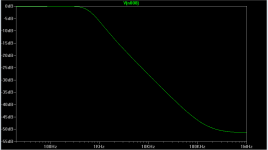
The plot of supply impedance (seen from the pov of the powered opamps, normalised to 2.5ohms) looks like this :
So I went over to Mouser to see what they have in lower ESR capacitors, and they have these : RR71C151MDN1 Nichicon | Mouser
I simulated these in conjunction with some TDK inductors (470uH, SLF 7mm range). There's a need for series resistance too as the Nichicons are just too good - without series R they'll have too high a Q. The additional series resistance turns out to be 1.5ohms, the inductors also have about 1ohm series R of their own.
The plot of supply impedance (seen from the pov of the powered opamps, normalised to 2.5ohms) looks like this :
Attachments
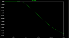
The plot of decoupling from the buffer's supply noise looks even better :
The downside of using through hole resistors is just board space and assembly time, no other reasons to go SMT.
As regards semiconductors being discontinued, its a business decision by TI to close a fab. Nothing particular to the LME parts.
The downside of using through hole resistors is just board space and assembly time, no other reasons to go SMT.
As regards semiconductors being discontinued, its a business decision by TI to close a fab. Nothing particular to the LME parts.
Attachments
You might even consider inductors in place of resistors.
To further reduce LF impedance, I played around with some inductors parallel to the series resistor, but I'm always a bit afraid of oscillations, when inductors are placed side by side to capacitors.
As the load is far away from the impedances involved in decoupling, the combination of series inductor and decoupling capacitor is basically an RLC circuit with R as inductor DC resistance.
Its damping factor is R_DC/2 * sqrt(C / L) and should be greater than 1 to prevent oscillations.
So there compete two requirements: If L is too low, it's far away from a notable series impedance, so the HF decoupling decreases. To meet at least 1 ohm @ 1kHz it should be >170uH.
But as L increases, I need additional series resistance (in series to the inductor, not only between the two caps) - internal as DC resistance or external. For L=200uH it should be at least about 0.3 ohms to be inconditionally stable.
I therefore looked for an inductor 220uH with about 0.5 ohms DC resistance:
TYS8040221M-10 Laird-Signal Integrity Products | 240-2755-1-ND | DigiKey
Simulations look good for that values:
An externally hosted image should be here but it was not working when we last tested it.
Just for comparance, the same inductance but with 30m ohms DC resistance:
An externally hosted image should be here but it was not working when we last tested it.
So (220uH + 0.5 ohms) || 10 ohms look very promising. But I'm not sure, whether it is worth the additional effort.
Do you think it is? Or should I just stick with 1 ohm series resistance?
<edit>
Seems you were a bit faster than me 😀
Last edited:
On the topic of electrolytic caps and their impedance characteristics, I made a rather interesting discovery a couple of days ago working on the power supply for my latest headphone amp - I just posted a rough schematic on my blog. That is that for higher voltage electrolytics (I have some 100V, 390uF ones, Korean brand) the corner frequency goes up. Its of no use to you in this design because those caps are too bulky but its another advantage of using transformers 🙂
The plot of decoupling from the buffer's supply noise looks even better
Yes, they really look promising!
And the choice of inductors looks good, too.
I'm just a bit cautious regarding the choice of caps. Polymere caps have really low voltage ratings. The best tradeoff I found was Nichigon 470uF 25V 15m ohms.
But I wonder if it is more wise to lower the edge frequency (by heading for 1000uF non polymere 35 m ohms) or to achieve real high decoupling for high frequencies.
With the former I achieve 28 dB @ 1kHz, 50 dB @ 3 kHz, 68 dB @ 10 kHz, with the latter 21 dB @ 1kHz, 45 dB @ 3kHz, 69 dB @ 10 kHz and with the cap you suggested 9 dB @ 1 kHz, 35 dB @ 3 kHz and 60 dB @ 10 kHz.
So maybe I should stick with the cap I currently use, would you agree?
If you worry about voltage ratings, run your opamps at 14V - the polymers I linked to are 16V rated. You originally said you were willing to forgo a volt on the rails to get decoupling - hence your 47R resistors.
15mohms won't have the HF rejection that the 7mohm ones I linked to have.
You'll need to weigh up to the two roles of the filter - the suppression of load-induced noise from the opamps themselves, and rejection of the buffer's load-induced noise. Of course the former becomes far less of an issue with higher feedback resistors.
What's the real estate taken by your 1000uF caps?
Sry if I'm just don't getting it, but I'm a bit confused now.
The data points I read from my simulations are just the rejection ratio from buffer's noise to the opamp power rail - so no noise from opamps themselves taken into account. (This would limit it to about 45 dB with 2k2 resistors and to about 78 dB with 100k resistors, but I got it, that I can raise this by far with higher feedback resistance. But I didn't take the opamps noise into account at all.)
I understood that the low ESR raises the frequency, where the filter is limited by the caps ESR. On the other side, the whole graph is pushed to higher frequencies by the lower capacity. So I tried to figure out, which effect is more dominant in the most sensitive frequencies - as you stated around 3 kHz. So i picked 1 kHz, 3 kHz and 10 kHz as representive points.
In my simulations the higher capacity has more decoupling effect in these frequencies than the lower ESR.
Or have I missed something?
No, I don't think you've missed anything. I agree that higher capacitance gives better buffer noise rejection - but higher capacitance also takes up more board space which I understood was at a premium. Hence my question about the real estate usage.
As regards the sensitive frequency, it was more an aside than a guide to choosing a capacitance value. I'd still be concerned about the performance up to 17kHz (my hearing certainly doesn't go any higher) because loop gain doesn't stop falling off at 10kHz.
As regards the sensitive frequency, it was more an aside than a guide to choosing a capacitance value. I'd still be concerned about the performance up to 17kHz (my hearing certainly doesn't go any higher) because loop gain doesn't stop falling off at 10kHz.
No, I don't think you've missed anything. I agree that higher capacitance gives better buffer noise rejection - but higher capacitance also takes up more board space which I understood was at a premium. Hence my question about the real estate usage.
I'm just a bit concerned, as f.e. the OPA1652 PSRR already rolls off at about 35 Hz, so it has significantly reduced in the most sensible areas.
But I admit: 15 kHz is also relevant, especially for brilliant details.
I therefore added a simulation for the effective PSRR, including a model of the PSRR (just an RC with a load, but models the datasheet precisely).
An externally hosted image should be here but it was not working when we last tested it.
So, you're right that it performes at bit worse >10 kHz, but as the PSRR rolls off that early, the frequencies to worry about are around 1 kHz.
But of course, this completely depends on the opamp used.
Fortunately both - cap and inductor - have the same footprint (not compared to each other, but the two variants), so I can choose them according to the opamp.
However, both variants completely outperform the variant with just a resistor:
An externally hosted image should be here but it was not working when we last tested it.
So the real gain is using an inductor (even with little series resistance) for additional decoupling.
So a very good idea 😉
Depending on the inductors you plan on using, it might be just as cheap and compact to use a pair of lm78l12/lm79l12.
Depending on the inductors you plan on using, it might be just as cheap and compact to use a pair of lm78l12/lm79l12.
Sounds good, too 🙂 The big advantage is the high decoupling for LF, whereas I already have a good PSRR there. At least, there would be no peak at about 300 Hz to 1 kHz in power line coupling.
On the other side, the voltage drop of 3V is on the verge to hurt, as the usable voltage range (for 12V power) gets down to about 5V peak. This especially applies to the input stage, as the source is 4 dBu line level with headroom up to 15 dBu (6.2V peak).
I just thought about adding a third/fourth PSU channel but I think, this would be a bit overblown.
One additional advantage of the inductor solution is that the LDO noise is additionally attenuated for HF. I didn't compare it to the input noise level, so I cannot say, if this makes a difference, but it is a nice bonus.
I will hurry to get the latest design online, as I'd be interested in which further ideas you have.
Sounds good, too 🙂
I had a look at the National DSs for those parts and found they're poorly characterized - so you have to make some educated guesses about how the 12V ones perform based on what they tell you about the 5V ones in the graphs.
Hello again 🙂
Sry for the long pause (>1 week), I have been very busy at work.
Besides this I did some redesign of the front-interface (also tightening the physical constraints to 45mm width and 90mm length) - you will see the jack moved a bit. But I freed the space below the jack (above the PCB) allowing to use it for the output caps - just the space over the jack (again above the PCB) keeps allocated for interfacing.
What did change since last time?
- Implemented abraxalito's suggestion relating power line decoupling (using inductor and series resistor) - it seems it fits the best for my situation
(Note: I used a 1206 resistor in between, but I finally switched back to a leaded one. It was physically best fitting as I had to cross the sound tracks anyway.)
- I implemented 00940's proposal of board design regarding the input stage opamp because it opens up many possibilities for reposition of the output filtering.
- Completely repositioned the output filtering as close as possible to the output jack
- Implemented 00940's solution for connecting the output jack ground to the actual amplifier stage
(Note: I used the pin header footprints but I just use the plated holes to solder the suggested twisted wire.)
Any comments on my implementations or additional tips from my two helpful advisors or anyone else who wants to help?
Sry for the long pause (>1 week), I have been very busy at work.
Besides this I did some redesign of the front-interface (also tightening the physical constraints to 45mm width and 90mm length) - you will see the jack moved a bit. But I freed the space below the jack (above the PCB) allowing to use it for the output caps - just the space over the jack (again above the PCB) keeps allocated for interfacing.
What did change since last time?
- Implemented abraxalito's suggestion relating power line decoupling (using inductor and series resistor) - it seems it fits the best for my situation
(Note: I used a 1206 resistor in between, but I finally switched back to a leaded one. It was physically best fitting as I had to cross the sound tracks anyway.)
- I implemented 00940's proposal of board design regarding the input stage opamp because it opens up many possibilities for reposition of the output filtering.
- Completely repositioned the output filtering as close as possible to the output jack
- Implemented 00940's solution for connecting the output jack ground to the actual amplifier stage
(Note: I used the pin header footprints but I just use the plated holes to solder the suggested twisted wire.)
An externally hosted image should be here but it was not working when we last tested it.
Any comments on my implementations or additional tips from my two helpful advisors or anyone else who wants to help?
- Status
- Not open for further replies.
- Home
- Amplifiers
- Headphone Systems
- DIY Headphone Amp - Comments and advice appreciated