Oops, yeah that's what I meant to say... Boyz. 
Thanks for the good suggestions. I'll probably refine a little more before sending out to board shop.
Thanks for the good suggestions. I'll probably refine a little more before sending out to board shop.
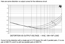
Going back to Nelson's description on Page 1. and looking at the distortion versus output voltage curve..
How does the gain chosen change the curve shape?
For example, does the shape remain the same and the curve move `down and to the left' at lower gain and is there anything you can do to stave off the dramatic rise in distortion with higher voltage output aside from paralleling multiple devices?
and
My understanding is that the devices that form the differential amplifier have to be matched, but a pair of devices within an individual `dual' like the LSK389 are intrinsically matched (or at least similar enough). My question is; if you parallel two (or more) dual devices in a LTP, so that `one half' of each critter is on either side of the LTP, then do you need do you need to match all the devices together or is it enough that there is a match left to right across both legs of the differential amplifier? i.e. can you parallel up multiple duals to reduce distortion without matching?
I appreciate I am asking to be spoon fed and there will be those whose kneejerk reaction might be to say `go build it and come back and let us know', but I am hoping someone feels the urge to partake in a teaching moment for their own joy and knowing that it is appreciated. I will further say that I miss the earlier descriptive essays that Nelson posted with every new gift of inspiration and ideas. I am limited to `cutting and pasting' and `slinging solder' and although there is a joy to be had in listening to something you have built, there is greater fascination (for me), in the conceptual arguments that underscore each new topology. But baby steps...
Yep, you'll have to match 'em if paralleling. The testing I did on my LSK389 showed good match between the dual sides. None of the 6 I have mated well device to device though.
As expensive as the K389's are, you might look at paralleling 2SK2145 (like Zen Mod famously does). You can get qty 100 for $46.
Lots of work testing those little buggers, but kind of fun too. You have to watch the each side of the dual match too, they don't always match.
Too bad the store doesn't sell octets of LSK170s. That way a builder could buy a set for each channel and just solder in... that would lower distortion!
Last edited:


I've never paid any attention to the tin/lead or lead/free packaging of resistors when ordering redidtors.
So, I've probably got a mix of both on my previous Pass builds. Now I'm concerned about this as I use
lead based solder. Just what might happen to my previous builds?
So, I've probably got a mix of both on my previous Pass builds. Now I'm concerned about this as I use
lead based solder. Just what might happen to my previous builds?
Danged Greedy B-words snapping up all the DIY FE 2022 Kits from the store in under 12 hours. 😳
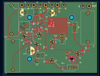
So I went ahead and laid out a version for myself so as to use some LSK389's I already have on-hand. Gives me more practice using KiCAD.
I just used Pa's PCB component arrangement, plopped the LSK389 in the middle and routed to my liking.
I may be a Copy Cat, but at least I'm not a Greedy B-word.
I guess I won't be getting a Holiday card from Cinco this year...🙁
Last edited:
Any idea what happens with 4 2SK170 parallel instead of 2 at the input ? will it work ?BeardyWan- I tried to fix the scaling on the article to better see the difference side by side in distortion between a gain of 10 and unity gain. There you more easily see the effect of increasing the negative feedback.
The best result at any gain level will be a quad of tightly matched K170's. I did that in my example at post #451. But that shouldn't stop anyone from building the FE '22 as it comes from the DiyAudio store (with the J113's), in my opinion. It will still sound great.
Last edited:
Probably wasting them. Remember this from the article?Any idea what happens with 4 2SK170 parallel instead of 2 at the input ? will it work ?
Attachments
Nothing. Lead solder is fine for Pb-free use.I've never paid any attention to the tin/lead or lead/free packaging of resistors when ordering redidtors.
So, I've probably got a mix of both on my previous Pass builds. Now I'm concerned about this as I use
lead based solder. Just what might happen to my previous builds?
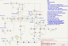
Here is my preliminary board layout. (Lots of checks yet to do!) This adds a MOSFET follower and has other mods to keep parts within their ratings. (This is to increase output to be able to drive a SIT OS, or other such options.) Alternately, a few jumpers and tack soldering a KSA992 onto this Q2 SMD footprint should allow the standard NP circuit to be built on same layout. No alternate footprints deemed necessary.
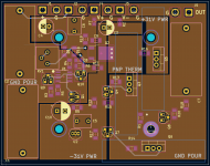
4-layer board stack:
1. Top (red traces)
2. GND plane (green)
3. Various pours including a thermal pad for Q2 as overkill (brown)
4. Bottom (blue or light traces)
TO-220 heat sinks are shown by the large rectangular outlines. One may be blocking a mounting hole access. Thinking that one over. The heatsinks maybe are not needed anyway.
Two interesting design options:
A. When testing my buffer, I realized it might be interesting to leave it outside the feedback loop. Zero ohm jumpers leave that option open.
B. Around the same time, I wondered what the effect of having a second J113 in the follower circuit might be, where the signal path mirrors the cascade current source. (See dwg here.) I tested and found it increased THD by almost 10x, from <0.01% to something approaching 0.1%. However, it was almost purely 2nd harmonic. I decided to leave that selectable via zero ohm jumper. (@Mark Johnson, I kept the 1 ohm set resistor, if for no other reason than easy current monitoring.)

Comments, especially on using an extra JFET in the follower stage, would be most welcome.
4-layer board stack:
1. Top (red traces)
2. GND plane (green)
3. Various pours including a thermal pad for Q2 as overkill (brown)
4. Bottom (blue or light traces)
TO-220 heat sinks are shown by the large rectangular outlines. One may be blocking a mounting hole access. Thinking that one over. The heatsinks maybe are not needed anyway.
Two interesting design options:
A. When testing my buffer, I realized it might be interesting to leave it outside the feedback loop. Zero ohm jumpers leave that option open.
B. Around the same time, I wondered what the effect of having a second J113 in the follower circuit might be, where the signal path mirrors the cascade current source. (See dwg here.) I tested and found it increased THD by almost 10x, from <0.01% to something approaching 0.1%. However, it was almost purely 2nd harmonic. I decided to leave that selectable via zero ohm jumper. (@Mark Johnson, I kept the 1 ohm set resistor, if for no other reason than easy current monitoring.)
Comments, especially on using an extra JFET in the follower stage, would be most welcome.
Attachments
Would a 2SK2145 dual jfet be a good part to use for the Q1/Q2 pair? Toshiba parts, matched pair, cheap ($.60 each), marked as audio specific, tens of thousands in stock... I suspect there must be a problem with using them for this amplifier or they would already have been discussed?
Attachments
Any clue when a new batch of kit will be in the store? I somehow missed the first batch.
Apologies if this is a recurring question. I signed up for the auto notification.
Apologies if this is a recurring question. I signed up for the auto notification.
Would a 2SK2145 dual jfet be a good part to use for the Q1/Q2 pair? Toshiba parts, matched pair, cheap ($.60 each), marked as audio specific, tens of thousands in stock...
2SK2145 is NOT a matched pair. No level of matching specified in datasheet. And I would always measure before use :
https://www.diyaudio.com/community/threads/2sk2145-matching-statistics.371427/
Patrick
measure of symmetry is matter of personal preferences/final goal
it tends to sharpen with increase of investment, both of resources and will
so, you can't compare goodness of something as you look at it and as regular Greedy Boy is looking at it
it tends to sharpen with increase of investment, both of resources and will
so, you can't compare goodness of something as you look at it and as regular Greedy Boy is looking at it
Did I say anything about level of symmetry or impact on circuit performance ?
Someone used the word "matched pair".
And I only gave a reponse based on real measurements.
All quantifiable, based on facts.
Nothing more, nothing less.
Cheers,
Patrick
Someone used the word "matched pair".
And I only gave a reponse based on real measurements.
All quantifiable, based on facts.
Nothing more, nothing less.
Cheers,
Patrick
Would you be able to listen to distinguish blindly a and b which circuit equips 2sk170 or 2145?
Would you be able to hear the difference between the J113 and 2sk170 version? Or between .0015 and .001% distortion? 🧐
Nelson has tried both and there are 6dB difference in between, as he posted earlier.
What you can or cannot hear I cannot judge.
There are people with golden ears.
And yes, we can tell the difference between a UDNeSS with J13 from one with dual 2SK209's.
But if distortion is unimportant, wouldn't the early ZEN versions be your favourite amp ?
Cheers,
Patrick
What you can or cannot hear I cannot judge.
There are people with golden ears.
And yes, we can tell the difference between a UDNeSS with J13 from one with dual 2SK209's.
But if distortion is unimportant, wouldn't the early ZEN versions be your favourite amp ?
Cheers,
Patrick
- Home
- Amplifiers
- Pass Labs
- DIY Front End 2022