😀Thanks Nic,
But...Rdegen trick comes at a price....slightly higher distortion, read this somewhere !, and according to Patrick ( EUVL ) deviating from 5R1 is to be avoided.
I fail to understand this but then that will be because i don't know enough of the subject.
My reasoning was in line with what you just laid out, the lower the Rdegen needed the better i thought. 5R1 being an average value.
I'd love to get the facts on this.😕
I think the idea of the trick is to lower distortion at the cost of higher local feedback (degeneration).
I am quite sure Patrick picked 5R1 because this is a value that "in average" will yield most NP-matches.
Maybe lower is better, but remember that there is already 11R is series in the F5X.
I think having different Rdeg for each J74 is a DIY'er luxury which can only be recommended😎
Anyway - wrong thread.
System the principle of measuring voltage as shown below.Example measure the Vbe,
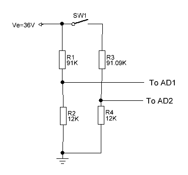
The BE two points of the voltage applied to the ADC input after 91K/12K resistor divider.
If R1/R2 and R3/R4 do not match. R1/R2=91K/12K R3/R4=91.09K/12K
When close sw1, Real Vbe is 0V. But because the resistor no match,The voltage difference between the AD1 and AD2 is
36* (12/(91+12) - 12/(91.09+12))=3.66mV
The system according to the measured, and then multiplied by the coefficient of the resistor divider, and it consider the Vbe voltage is:
3.66mV * (91+12)/12=31.4mV.
So if you measure the JFET Vgs-Id curve, system consider Vgs=0, But in fact the voltage of G/S is not zero.
This error voltage will change with the ground voltage (V) varies.
And when you measure N type ,the Ve is set to 2.5V,and measure the P type,the Ve will set to 36V. So At difference Ve,the error voltage is no same.
So I used some correction algorithm, possible error voltage Ve = 2.5 to 36V range to minimize.
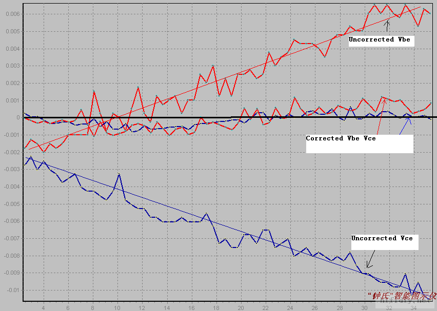
The following diagram is shorted BE and shorted CE,and show Vbe / Vce voltage curve under different Ve.
The BE two points of the voltage applied to the ADC input after 91K/12K resistor divider.
If R1/R2 and R3/R4 do not match. R1/R2=91K/12K R3/R4=91.09K/12K
When close sw1, Real Vbe is 0V. But because the resistor no match,The voltage difference between the AD1 and AD2 is
36* (12/(91+12) - 12/(91.09+12))=3.66mV
The system according to the measured, and then multiplied by the coefficient of the resistor divider, and it consider the Vbe voltage is:
3.66mV * (91+12)/12=31.4mV.
So if you measure the JFET Vgs-Id curve, system consider Vgs=0, But in fact the voltage of G/S is not zero.
This error voltage will change with the ground voltage (V) varies.
And when you measure N type ,the Ve is set to 2.5V,and measure the P type,the Ve will set to 36V. So At difference Ve,the error voltage is no same.
So I used some correction algorithm, possible error voltage Ve = 2.5 to 36V range to minimize.
The following diagram is shorted BE and shorted CE,and show Vbe / Vce voltage curve under different Ve.
Attachments
The 2sa970 component foot is right?
Send the save data(.cuv) to me.
When start the measurement, the system control 3 channel output only moment of voltage.
When measure finish, 3 channel output to 0.
If you want to measure 3 channel output voltage by DMM, you can select menu 'option->diagnoosis' and 'Device Test' page -> 'Voltage Test' box,
Set the 3 channel output voltage and click the 'Output' button,
Then you can get the static voltage.
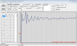
I locky-z, thanks for the reply. This is the screen shot for the 2sa970: I alyways get very low hfe I do not not know to send the .cuv file.
The 2sa970 component foot is right?
Send the save data(.cuv) to me.
When start the measurement, the system control 3 channel output only moment of voltage.
When measure finish, 3 channel output to 0.
If you want to measure 3 channel output voltage by DMM, you can select menu 'option->diagnoosis' and 'Device Test' page -> 'Voltage Test' box,
Set the 3 channel output voltage and click the 'Output' button,
Then you can get the static voltage.
Attachments

I locky-z, thanks for the reply. This is the screen shot for the 2sa970: I alyways get very low hfe I do not not know to send the .cuv file.
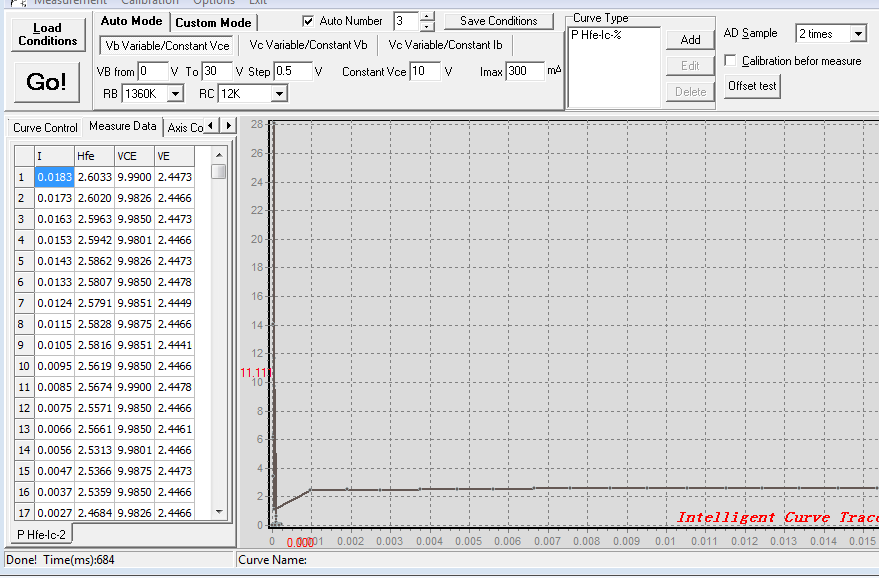
The NPN (2sc2240) test seems to be ok!
Attachments
2SA970 you need to load the 'PNP Ic-Hfe' condition.
PNP's voltage is negative.
It is what I did. I tried 3 different types of PNP transistors with always the same problem: hfe = 2 to 3. Again, The NPN test is OK as you can see on the picture! Could something be wrong with the board? Unfortunately I cannot aford to spend days to fix. Any suggestion will help, thanks

OK I see! I was thinking that the load condition would set up the polarity automaticaly!
I have to learn but I anticipate this tool to be very useful for me. Thank you for your patience!
I have to learn but I anticipate this tool to be very useful for me. Thank you for your patience!
The PNP measure condition is:
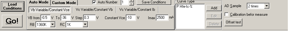
But from your picture,I think your condition is NPN type.
Normaly in PNP's result data,The Vce is negative, Ve is +35~36V.
Hi locky_z,
Everything works fine except that the first load condition ''PNP IC>Hfe (fix VCE)''
does change nothing so I have to enter the values manually but it is ok.
I have tested some rare parts like NEC 2sd188/2sa617, and other bipolars or power mos at 2 Amp, small bjt and jfet complementary pairs for matching.
It's a piece of cake and a real game! Also, I measured IDDS=3.61 mA, VGS=0 with the curve tracer for some 2sk30 where the battery test gives 3.54 mA with G-S short circuited, which is not bad. Anyway I need relative datas rather than absolute.
Thanks a lot.
To measure the Idss accurately, I suggest load the measure ‘diode condition ’.
You can short the G-S and as a diode connect to C/E socket
You can short the G-S and as a diode connect to C/E socket
Hi locky_z
I wanted to purchase the intelligent curve tracer from ebay. I live in the US and want to carry out some analysis on my devices. If i would purchase, what would would supply as a whole kit. Do you supply the whole box or some parts have to be assembled. Also do you supply a manual or a CDROM along with the purchase?
Thanks a bunch
The ‘Intelligent Curve Tracer on ebay’ is a whole box, you just connect it to 100~240VAC power and run the software on pc.
The ‘Curve Tracer mainboard on ebay’ is only a welding board, you need addition DC power supply / heat sink / shell.
If you purchase them ,the manual and software will send to you by email.
The ‘Curve Tracer mainboard on ebay’ is only a welding board, you need addition DC power supply / heat sink / shell.
If you purchase them ,the manual and software will send to you by email.
Hi,
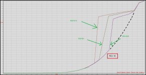
I have have been trying to test small mosfets but i keep getting those strange curves.
I suspect there may be an issue with the equipment, so i`m asking for your advice.
The part being tested is ZVN3310A mosfet.
You see, the dotted line i marked is like a logical continuation of the curve, The discontinuation looks like an error of some kind..
I may be overlooking something.. ??
Thank you all.
Attachments
Last edited:
It look like oscillation occur, you try connect a 10n ~ 100n capacitor parallel FET D-S. and try again.
And give me the save curve data file.
And give me the save curve data file.
True.
But even easier:
1) Trace all the FETS without any kind of degeneration.
2) From the traces sort and record Id @ 0V and 0.1V
3) Copy to excel (and fix all the stupid decimal and errors😡)
4) Calculate Yfs = (Id@0V-Id@0.1V)/0.1V
5) Recalculate Idss and Yfs for the J74 using selected Rdeg values (I use 4R3, 4R7, 5R1, 5R6, 6R2, 6R8 and 7R5).
Congratulations! - you now have 7 times as many J74 devices to choose from😀
6) Match you K170 and degenerated J74 devices for both Idss and Yfs.
7) Remeasure (or trace) the pairs/sets you have identified, but now with degeneration and be ready for a pleasant surprise😎
Hi Nic,
Thanks for these tips, but I think I need some help to understand.
Can you please detail the setting/condition you used for J74 and K170 (which load condition and if you changed any variables).
For point (5), what is the formula to recalculate Idss and Yfs using Rdeg?
For point (7), how do you curve trace with degeneration?
- Status
- Not open for further replies.
- Home
- Amplifiers
- Solid State
- DIY Curve Tracer for PC