Hello,
This is my recent project I still work on. It's current-mode R-2R DAC module with 0,1% resistors, but with fairly good results (see below).
24-bit resistor network is divided into three 8-bit segments, with fine-tunable reference voltage for lower two segments, in order to get best linearity with used resistors.
It doesn't have any programmable parts, just regular components that anyone can buy and solder on PCB.
For my prototype I use I2SoverUSB as digital interface. I2S lines are connected to DAC board, and output is filtered analog signal with 2 Vrms full scale output.
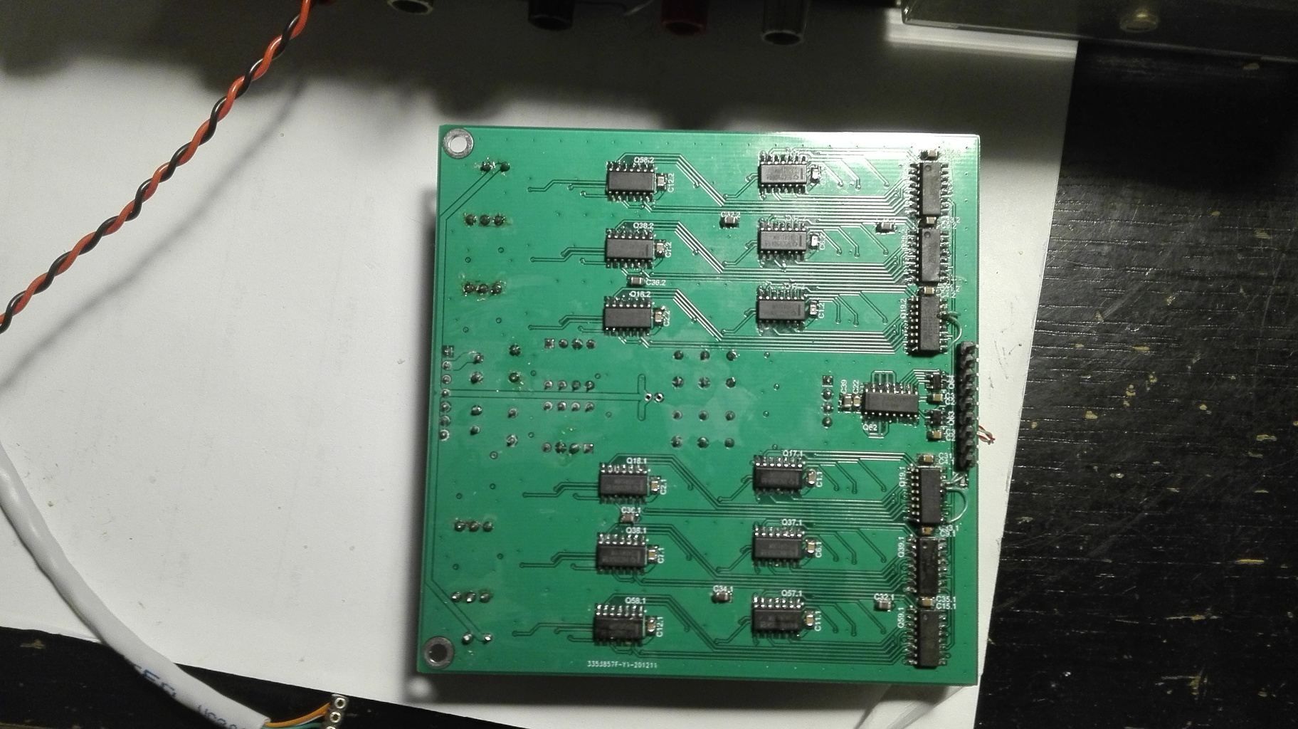
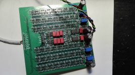
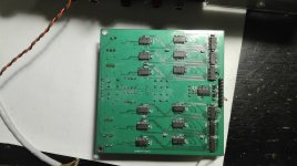
At first, I made just board with digital logic for ladder driving, resistor ladder, I/V converter, and low-pass filter, (picture bellow). But, it showed up that sample and hold circuit is required for deglitching, so I made it as additional smaller board.
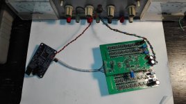
This is how it looks:


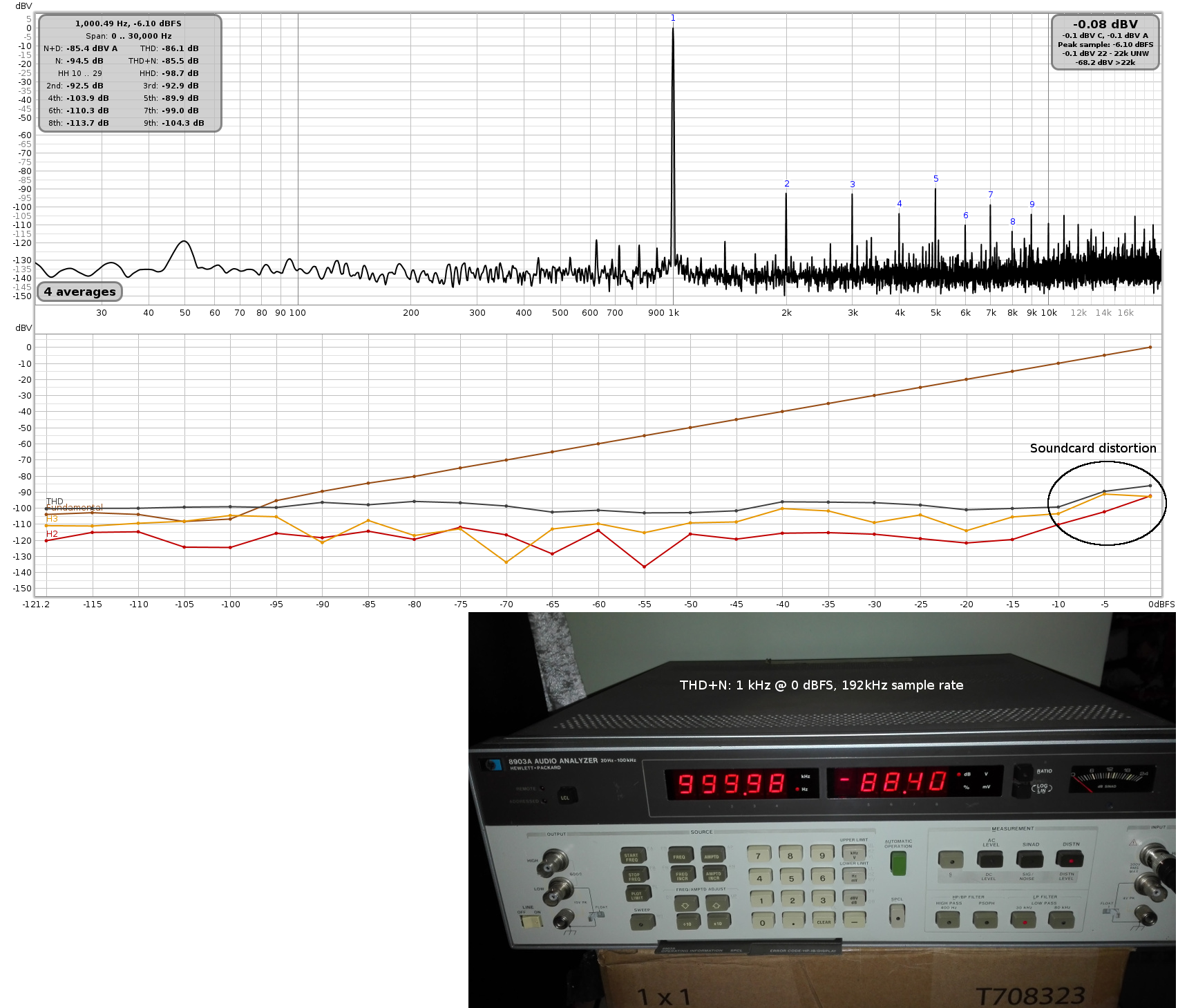
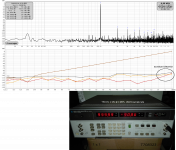
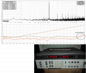
And this is what i get:
Left channel THD:

Right channel THD:
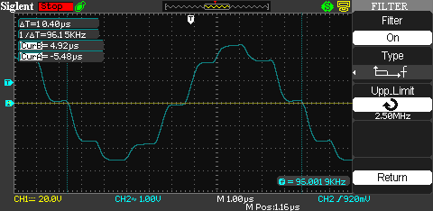
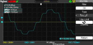
96 kHz signal at 768 kHz sample rate, at S/H circuit output
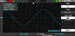
At low-pass filter output:

2nd order 40 kHz Butterworth filter
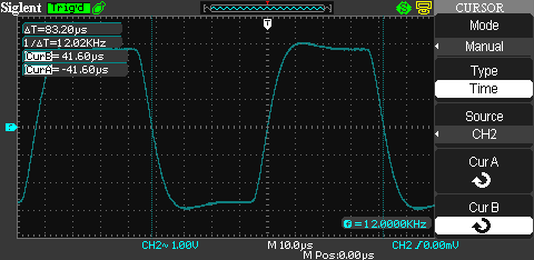
12 kHz square wave signal, at low-pass filter output
Complete schematic is not a secret, but it's still a work-in-progress
This is my recent project I still work on. It's current-mode R-2R DAC module with 0,1% resistors, but with fairly good results (see below).
24-bit resistor network is divided into three 8-bit segments, with fine-tunable reference voltage for lower two segments, in order to get best linearity with used resistors.
It doesn't have any programmable parts, just regular components that anyone can buy and solder on PCB.
For my prototype I use I2SoverUSB as digital interface. I2S lines are connected to DAC board, and output is filtered analog signal with 2 Vrms full scale output.
At first, I made just board with digital logic for ladder driving, resistor ladder, I/V converter, and low-pass filter, (picture bellow). But, it showed up that sample and hold circuit is required for deglitching, so I made it as additional smaller board.
This is how it looks:
And this is what i get:
Left channel THD:
Right channel THD:
96 kHz signal at 768 kHz sample rate, at S/H circuit output
At low-pass filter output:
2nd order 40 kHz Butterworth filter
12 kHz square wave signal, at low-pass filter output
Complete schematic is not a secret, but it's still a work-in-progress
Attachments
-
 IMG_20201227_095832.jpg690.7 KB · Views: 3,802
 -
 IMG_20210211_063338.jpg627 KB · Views: 2,960
 -
 IMG_20210220_155105_2.jpg599.9 KB · Views: 3,007
 -
 L_thd_all.png744.8 KB · Views: 2,847
 -
 R_thd_all.png743.4 KB · Views: 2,787
 -
 96khz_na_768khz_sh-out.png7 KB · Views: 2,858
 -
 96khz_na_768khz_lpf-out.png6.5 KB · Views: 2,839
 -
 12khz_lpf.png7.2 KB · Views: 2,789
Last edited:

Hi enaB,
Are you using discrete transistor as the R2R switches? Would you tell us the part number?
Are you using discrete transistor as the R2R switches? Would you tell us the part number?
Are all this with a 24bit PCM input signal?
//
Yes. I had to add one more shift register on top of the other for each channel, to hold whole 64-bit I2S frame. It's barely visible on second picture
Sure 🙂 BSS119NHi enaB,
Are you using discrete transistor as the R2R switches? Would you tell us the part number?
can you measure it with 16 bit test signal ?
Would it even accept a 16 bit signal? I don't see how.
Yes, but I cannot set REW to use 16-bit signal to do a level sweep.can you measure it with 16 bit test signal ?
At -60 dBFS there is no difference, and at 0 dBFS THD+N is about 0.5 dB lower (better) with 16-bit signal (lowest 8 bits not switching) than with 24-bit signal. Measured at 192 kHz sample rate
Of course it would, digital interface gives a fixed frame format I2S (32 bits per channel) with zero padded lower bits.Would it even accept a 16 bit signal? I don't see how.
Here is the schematic. It is mostly redrawn to include all changes made on PCB, so I don't guarantee that there isn't some overlooked drawing mistake.
Attachments
current-mode R-2R DAC module with 0,1% resistors, ...24-bit resistor network is divided into three 8-bit segments, with fine-tunable reference voltage for lower two segments, in order to get best linearity with used resistors.
Brilliant design. Any updates please?
Thanks! Not much, it's on hold. The last thing I worked on was trying different voltage filtering and regulation designs for supply and reference voltage. It measures the same, but the sound is different.
Interesting. I wonder if there's an explanation?It measures the same, but the sound is different.
I've been thinking about a discrete R-2R DAC myself for some time, but have not got further than a paper design. Kudos to you for going all the way to a working prototype!
Some questions:
1. Did you consider doing a differential output from the R-2R ladder, instead of switching to ground?
2. Is the reason for discrete transistors for switches the increased VREF voltage? Did you consider the 1G3157 or similar?
3. With this design the linearity is very dependent on the trimming of R97 isn't it? How about a sign-magnitude implementation? Have you thought about testing your 2-channel DAC as a mono sign-magnitude DAC?
Small frequency dependent coupling of opamp supply and reference voltage is one possibility I think.Interesting. I wonder if there's an explanation?
Thanks!I've been thinking about a discrete R-2R DAC myself for some time, but have not got further than a paper design. Kudos to you for going all the way to a working prototype!
Some questions:
1. Did you consider doing a differential output from the R-2R ladder, instead of switching to ground?
2. Is the reason for discrete transistors for switches the increased VREF voltage? Did you consider the 1G3157 or similar?
3. With this design the linearity is very dependent on the trimming of R97 isn't it? How about a sign-magnitude implementation? Have you thought about testing your 2-channel DAC as a mono sign-magnitude DAC?
1. I don't remember. I consider it now, and I would not change it. Vref should be precise and stable in respect to that input, and the input offset of I/V converter should be trimmable, so it is simpler to just ground other side.
2. I considered similar analog switches, but I wanted make-before-break switching to minimize glitches, and simple, monotonic switch resistance characteristic. Many analog switches combine N and P FET-s and have dips and bumps in combined resistance characteristics. In addition to low on-resistance, high speed, and low gate capacitance.
3. Well, yes, but it is equally important as in the sign-magnitude design, isn't it? This design have only one network to trim, sign-magnitude have two to be trimmed and matched, which increases the total number of precision resistors and the price. However, sign-magnitude have one big advantage, and that is a low number of switching transistors on low digital signal level so gate charge injection noise is low. This one current mode network design have very audible switching (charge injection) noise on low digital signal level without sample-and-hold circuit to "hold" over a short transition period. This is the reason I added 15 pF capacitors too, to compensate gate capacitance and minimize charge injection.
Thank you for the explanation, seems like reasonable tradeoffs. I was wondering about those 15p caps too.
Very impressive with lots of generous and useful details. THANKS.
As a side note, I have been searching for this "sign-magnitude" design for a while - with no success. Could anybody supply some info/links on how it works and implemented?
As a side note, I have been searching for this "sign-magnitude" design for a while - with no success. Could anybody supply some info/links on how it works and implemented?
Thank you guys, I'm glad that you like it!
@murat
I think I stumbled upon some patent or application note for "sign-magnitude" at some moment, but I can't find it now.
I didn't want to write about sound, it is a very subjective topic and I don't know how to describe it properly, but if you wish... 🙂 I didn't expect Vref source to have a great impact on sound in this current-mode R-2R topology, but it seems that it has. I did all my earlier tests with the old regulated supply (not audio grade 🙂 ) for +15V (Vcc) and -15V voltage for analog circuitry, and Vref derived from Vcc (VANP in the schematic) by connecting Vref to Vcc via one blue LED diode, just to have lower voltage on Vref (this R-2R network sinks constant current on Vref). This sounded quite well in my opinion. Slightly narrower than my CDP-710 player with TDA1541A(+NE5532) or DAC with PCM1794A(+LME49710) I made earlier, but tonally I liked it better. CDP has a more colored sound, this R-2R sounded more natural to my ears.
Changing LED diode with pure resistance (a few hundred ohms or so), and forming just a simple RC filter on VREF from Vcc, the sound stage gets very wide, but the sound was somehow...diluted, and vocals get far in front of me, presence is lost.
I need to make a proper power supply with independent voltage regulators for every voltage level, and then continue experimenting to get as much as I can from this.
Gerber files needs revision, I can share them when I finish the project.
- Home
- Source & Line
- Digital Line Level
- DIY 768 kHz 3x8b segmented current mode R-2R DAC module