Hello dear diyAudio people,
during the last months I 'designed' a discrete headphone amplifier. I designed some pcbs and tested them. The amplifier is okay for our needs and sounds somehow good enough. But I am wondering why there is a resonance peak in the frequency response at very high frequencies with a connected inductive load.
the figure below shows the amplifier schematics. It is inspired by the classical 'blameless amplifier' from Douglas Self.

Here you can see the frequency response of the amplifier with the inductance connected (the inductance is simulating our headphone load).

However. I designed the amplifier without an inductive load in my mind and with the indicator shorted everything looks fine:

So now my question is. Does anyone how has plenty more amplifier knowledge than me, where this resonance peak is coming from within the circuit?
I mean at this point I have now idea 0.o
so thank you 🙂
Cheers
Gruftgrabbler
during the last months I 'designed' a discrete headphone amplifier. I designed some pcbs and tested them. The amplifier is okay for our needs and sounds somehow good enough. But I am wondering why there is a resonance peak in the frequency response at very high frequencies with a connected inductive load.
the figure below shows the amplifier schematics. It is inspired by the classical 'blameless amplifier' from Douglas Self.
Here you can see the frequency response of the amplifier with the inductance connected (the inductance is simulating our headphone load).
However. I designed the amplifier without an inductive load in my mind and with the indicator shorted everything looks fine:
So now my question is. Does anyone how has plenty more amplifier knowledge than me, where this resonance peak is coming from within the circuit?
I mean at this point I have now idea 0.o
so thank you 🙂
Cheers
Gruftgrabbler
Attachments
Try putting a capacitor across R96. The feedback network has to charge Q18's base which is not unlike a capacitor shunting the feedback input. It doesn't help that you are using equal 10k feedback resistors which is the worst scenario for feedback divider impedance. Discrete BJTs don't have low capacitance and input current like modern audio opamps do, so they don't tolerate 5k feedback impedance like an opamp might.
And with a nominal gain of 2 you are pushing the upper cut-off frequency very high. This means it has a feedback path still operating when the phase shift caused by the delay as KT says adds an unwanted response. If a capacitor alone does not work you could try using a CR network (such as 10nF-1k) across both the feedback resistor and the associated grounding resistor. This may introduce a slight freuquency bump if the components are not accurately matched, so 1% resistors and as tight a tol caps as possible. This will maintain the low frequency impedance at 5k but bring the high frequency impedance down to 500 ohms.
Another thing you can try is a CR network on the output to offset the inductance. Commonly known as a Zobel network it is only a true one if the impedances match. I suspect a 30 ohm load (to match the headphone impedance) and a 47nF would work (around 100kHz) might be sufficient to make the load appear resistive enough to give the amp a better chance with its phase margin, but maybe 22nF would also work if you want a better response.
Another thing you can try is a CR network on the output to offset the inductance. Commonly known as a Zobel network it is only a true one if the impedances match. I suspect a 30 ohm load (to match the headphone impedance) and a 47nF would work (around 100kHz) might be sufficient to make the load appear resistive enough to give the amp a better chance with its phase margin, but maybe 22nF would also work if you want a better response.
Hello dear diyAudio people,
during the last months I 'designed' a discrete headphone amplifier. I designed some pcbs and tested them. The amplifier is okay for our needs and sounds somehow good enough. But I am wondering why there is a resonance peak in the frequency response at very high frequencies with a connected inductive load.
the figure below shows the amplifier schematics. It is inspired by the classical 'blameless amplifier' from Douglas Self.
View attachment 1016886
Here you can see the frequency response of the amplifier with the inductance connected (the inductance is simulating our headphone load).
View attachment 1016888
However. I designed the amplifier without an inductive load in my mind and with the indicator shorted everything looks fine:
View attachment 1016891
So now my question is. Does anyone how has plenty more amplifier knowledge than me, where this resonance peak is coming from within the circuit?
I mean at this point I have now idea 0.o
so thank you 🙂
Cheers
Gruftgrabbler
There is no detail on voltage supplies or circuit voltages if the supply rails are low the collector to base capacitance in Q6 will be high since the value varies in inverse proportion to the square root of the voltage applied at the collector.Hello dear diyAudio people,
during the last months I 'designed' a discrete headphone amplifier. I designed some pcbs and tested them. The amplifier is okay for our needs and sounds somehow good enough. But I am wondering why there is a resonance peak in the frequency response at very high frequencies with a connected inductive load.
the figure below shows the amplifier schematics. It is inspired by the classical 'blameless amplifier' from Douglas Self.
View attachment 1016886
Here you can see the frequency response of the amplifier with the inductance connected (the inductance is simulating our headphone load).
View attachment 1016888
However. I designed the amplifier without an inductive load in my mind and with the indicator shorted everything looks fine:
View attachment 1016891
So now my question is. Does anyone how has plenty more amplifier knowledge than me, where this resonance peak is coming from within the circuit?
I mean at this point I have now idea 0.o
so thank you 🙂
Cheers
Gruftgrabbler
Due to Miller effect this capacitance which is non linear will be amplified along with that of C12 the external capacitor which has to be sufficiently large to swamp the non-linear element in Q6 and presented as a load for the LTP to drive.
The tail current of this is about 6 m.a. roughly double what to expect in a power amplifier, however at 1nf the value of C12 is about ten times what might suffice in a power amplifier.
Also Q17 and Q19 are have their collectors connected to their respective bases to act as diodes. This is a fixed bias arrangement with no means of adjustment for the output transistors standing current - to be sure there is enough measure the voltage drops across the 4R7 output transistor emitters and deduce from Ohms law. You don't want to be running this close to Class B
your answers were great and I managed to get rid of the peak without modifying the pcb with replacing the dominant pole capacitor C12 with a 10nF cap. The resonance peak is away. Of cause the slew rate is heavily affected and slew limiting occurs now at around 30kHZ which is quite bad. But this is a topic for the future and another generation of the pcb. In the next generation I will definitively increase the closed loop gain the help reduce the pole, so thanks!
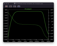
Ähm, but there still one think I do not really understand. I measured the frequency response of the pcb with matched input transistors and a headphone load with around 30Ohms resistance and 60uF of inductance. The given plot of the frequency response is in the figure below.
As you can see the peak is mostly gone, but not complete. BUT the -3dB Cutoff Frequency is in the real measurement at around 60kHz.

in the simulation you can clearly see that the cutoff frequency is at something like 1Mhz (with 10nF C12 and 30ohms resistance as load and 60uF inductance)

But however. If I probe in the simulation at the point NFB I get a -3dB cutoff of around 100kHZ which is at least in the order of the real measurement. But the real measurement is not taken at the point NFB it is taken right before the headphone, just like the first measurement.

At this point I really have to apologise for my stupid question. I feel like a complete noob, despite putting so much time into literature research, design and testing. I still missed this super important point!
So thanks and Cheers
Gruftgrabbler
Ähm, but there still one think I do not really understand. I measured the frequency response of the pcb with matched input transistors and a headphone load with around 30Ohms resistance and 60uF of inductance. The given plot of the frequency response is in the figure below.
As you can see the peak is mostly gone, but not complete. BUT the -3dB Cutoff Frequency is in the real measurement at around 60kHz.
in the simulation you can clearly see that the cutoff frequency is at something like 1Mhz (with 10nF C12 and 30ohms resistance as load and 60uF inductance)
But however. If I probe in the simulation at the point NFB I get a -3dB cutoff of around 100kHZ which is at least in the order of the real measurement. But the real measurement is not taken at the point NFB it is taken right before the headphone, just like the first measurement.
At this point I really have to apologise for my stupid question. I feel like a complete noob, despite putting so much time into literature research, design and testing. I still missed this super important point!
So thanks and Cheers
Gruftgrabbler
If your output bias is too low, your amp can appear much slower in the crossover region. The Oliver bias condition (~26mV per emitter resistor) is important for minimizing crossover distortion but also important for consistent bandwidth across the range of possible output currents.
Did you do a loopback test to make sure your setup has the BW needed for the test?
Did you do a loopback test to make sure your setup has the BW needed for the test?
In the simulation the standing current of the output stage is 4.2mA, so the voltage across the emitter resistance is about 19mV
In the real pcb I measured 27mV across the emitter resistors.
You think this small difference is causing the error???
In the real pcb I measured 27mV across the emitter resistors.
You think this small difference is causing the error???
A good many of your component values choices need to be rescaled. For example the constant current sources in the LTP and VAS stages are at the same level.In the simulation the standing current of the output stage is 4.2mA, so the voltage across the emitter resistance is about 19mV
In the real pcb I measured 27mV across the emitter resistors.
You think this small difference is causing the error???
R93 is far too low at 1k we don't know what the supply rail voltages are, supposing these are +/- 12V then 18k to 22k would be closer to the mark. The increased value of C12 at 10nF is a move in the wrong direction 220pF would be a more likely value. Also make R94 220 Ohms.
The output terminal of your amplifier should be within a few mV of dc. You have a series blocking capacitor which suggests otherwise.
For 30 Ohm headphones you will need medium power transistors like TIP31 and TIP32 for greater output current output capacity. To allow such the emitter resistors will should be no more than 1 Ohm.
The Vbe arrangement should provide a range of adjustment in setting the standing currents in these transistors.
Also follow John Ellis' advice on adding a zobel stability network to the output.
Q18 - the inverting input is a summing junction - signals to and from the load will be summed with those arising similarly in the pathway in the zobel network to earth.
thank you for all your help 🙂 Those tipps were super helpful!
I think in a week or so I go back into the books and do some re-reading again in order to learn from my mistakes.
I should've mentioned it before, but I am not free in choosing all components on this amplifier. I have to use the SMD BC807/BC817 and the THT BC337/BC327. I also have a lot of space restriction. The amplifier must be exakt 50mm x 10mm in size. Expect the 4.7 and 22 Ohms resistors every other resistor has to be a 0805 100,1k,10k or 100k resistors. No other resistors allowed. I also can use a SMD 10uF cap and a THT 220uF cap. C12 (C_dom) is free since there I can choose the footprint and size for the needs. And the amplifier is running at +-9V
So I am trying to make the best out of this all restrictions and deliver something okayisch. doesn't have to be hifi at all, since our signal sources aren't clean anyway.
However this makes it impossible to use a nobel network, or use special power transistors, because they have a much larger footprint.
So thank you again all and
Cheers
Gruft
- Home
- Amplifiers
- Solid State
- Discrete Amplifier Resonance Peak with connected Load