If your'e interest I've got a couple of suggestions for the latest revision:
* The gates of J8/J9 might better connect to the sources of J1/J2--this will greatly reduce the voltage dependence of input C and corresponding HF distortion if driven from a substantial source impedance.
* For J3-J7 I'd choose a different part with lower C. The low voltage noise of the 2SK170 is of little relevance here, but output Z is.
* T1 might be operated at 3 mA (the sum of T3 and T4 collector current) to approximately cancel the base current errors of T3/T4.
* As shown distortion performance is likely entirely dominated by voltage-dependent loading of the output stage. You can address this by driving the output stage from T1 emitter.
* The next step is to derive a cascode for T1 which will increase the Z at T6's collector, giving lower distortion and more open-loop gain.
* To reduce HF distortion further you could drive C7 from T1 emitter instead of T6 collector.
Samuel
I use it as a (somewhat) portable headphone amp. The original design was more or less a discrete AD829. I've later retrofitted stuff to it, so my amps look a bit messy. I use active ground. That's why there are 3 channels inside, and as virtual ground there's a TLE2426. It's powered by 8 AAA's, have a trickle charger and an L7818 regulator (temporarly removed). It's made for Hammond J1201, but they've become so expensive that I've made a couple of aluminium boxes.Nelson,
it might have slipped me, but how do you use this stage? As a preamp?
Did you try what happens using higher gains, soundwise?
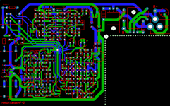
It would be quite interesting how you did the acutal layout of your circuit, do you happen to have any photos?
Rüdiger
I haven't tried it with higher gain, but it should be no problem to do so.
The layout is very tight because I wanted it to fit a back pocket. Resistors are tombstoned and some transistors had to be grinded down a bit to fit the board.
Attachments
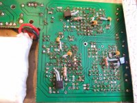
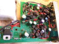
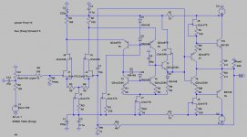
Like you can see on the pictures, there's little room for more mods, but I'll try to do this.If your'e interest I've got a couple of suggestions for the latest revision:
* The gates of J8/J9 might better connect to the sources of J1/J2--this will greatly reduce the voltage dependence of input C and corresponding HF distortion if driven from a substantial source impedance.
I ordered 100 pcs of SK170 so I could get perfect matches for the LTP, and I used the rest of them as current sources/sinks. This was the least costly option. Would 2N5486 be more appropriate?* For J3-J7 I'd choose a different part with lower C. The low voltage noise of the 2SK170 is of little relevance here, but output Z is.
I did some adjustments, so now it's 3 mA exactly.* T1 might be operated at 3 mA (the sum of T3 and T4 collector current) to approximately cancel the base current errors of T3/T4.
I've thought about this too. This is how it's done in LT1469. In LTSpice it shows a little bit higher 2nd and 4th but slightly lower 3rd. Do you think it would look like this in real life as well?* As shown distortion performance is likely entirely dominated by voltage-dependent loading of the output stage. You can address this by driving the output stage from T1 emitter.
Do you mean a cascoded emitter follower? In AD797 I think there's a double EF. This gives the right voltage drop. Should the cascode emitter connect to the collector of the first of them or both of them if a double EF is used?* The next step is to derive a cascode for T1 which will increase the Z at T6's collector, giving lower distortion and more open-loop gain.
This would be easy to try in this amp. Do you think there'll be an audible improvement?* To reduce HF distortion further you could drive C7 from T1 emitter instead of T6 collector.
Thank you very much for your interest Samuel. I'll see if I can implement some of this and come up with a new schematic.
I'm thinking of doing a speaker amp, so these tips might come in handy. The input stage will be inspired by "the memory distortion philosophies" with both cascode and CFP. This kind of AD797 VAS might be it or maybe a differential cascoded VAS. I really don't know what output stage I should use.
Would 2N5486 be more appropriate?
This looks like a decent part for your application. I don't want to talk you into endless mods, the effect is probably relatively small here. Perhaps more something if you're doing a new board revision anyway. In fact I think I'd use BJT sources as they offer larger voltage swing and don't need any adjustment. But of course up to you.
In LTSpice it shows a little bit higher 2nd and 4th but slightly lower 3rd. Do you think it would look like this in real life as well?
I would not trust SPICE too much at these distortion levels. Within the audio frequency range distortion of this topology mainly depends on the relationship of hFE to Ic and Early voltage to Vc. Particularly the later is not well simulated (actually: not at all!). What I can tell you is that even for two-stage amplifier topologies the loading of the output stage is typically a dominant distortion mechanism, particularly if the output current magnitude exceeds class A. And single-stage topologies are even more sensitive for this mechanism.
Do you mean a cascoded emitter follower? In AD797 I think there's a double EF. This gives the right voltage drop. Should the cascode emitter connect to the collector of the first of them or both of them if a double EF is used?
I don't have the full AD797 schematic at hand right now but I'm pretty confident that they use a more complex current mirror implementation where one emitter follower drives the bases of the current mirror transistors and the Darlington emitter follower acts as bootstrapping element. In this case you can either bootstrap only the second emitter follower of the Darlington pair (as it is done in the AD797) or all three collectors.
I'd say for your discrete implementation you're fine with the basic current mirror you use--transistor mismatch will anyway limit things pretty quickly, and the added complexity is significant. For the added cascode a JFET would be most simple.
This would be easy to try in this amp. Do you think there'll be an audible improvement?
Without looking at it in detail I guess the improvement happens at the top of the audio frequency range and above only. Perhaps it results in somewhat reduced RF sensitivity. Just make sure stability remains well.
Samuel
Did I understand you regarding the cascoded T1?
You can directly use a 2SK246 as cascode--tie the gate to the emitter, the source to the collector and the drain to the positive supply.
Samuel
And: I'd replace D3 with a 33 Ohm resistor. This operates T3/T4 at near-equal collector voltage which improves the balance of the current mirror. This assumes that the sum of the collector currents of T3 and T4 is equal to that of T1 as discussed above.
Ideally T1 would be cascoded such that its collector voltage is also equal to that of T3/T4, but that's not easily achieved without significant changes.
Samuel
Ideally T1 would be cascoded such that its collector voltage is also equal to that of T3/T4, but that's not easily achieved without significant changes.
Samuel
So with the tweaks suggested in this thread, it might look like this. Because of the added cascode, it wont be suitable for battery operation since I loose some swing. I could add parts to balance the VAS CM voltages, but it would take some work. Do you think it's worth it soundwise?
If I were to realize something like this, I should add trimpots to be able to adjust the VAS CM collector voltages and the current going through the CM and shunt transistor.
If I were to realize something like this, I should add trimpots to be able to adjust the VAS CM collector voltages and the current going through the CM and shunt transistor.
Attachments
T7/8 are heavily saturated in you last schematic...they work in sim, but in reality they probably won't...
I don't follow all changes you applied; D3-D5 should be replaced with a short, and R5 should be 33 Ohm. I don't think that bootstrapping of T7/T8 is necessary with the output stage drive from T1 emitter but if you do it it would be better to connect the collectors of T7/T8 to the emitters of T9/T10. Otherwise they might come close to saturation with low output loads.
You're right J10 might limit positive output swing. Skip it or use a BJT, but this requires some more biasing elements.
Samuel
You're right J10 might limit positive output swing. Skip it or use a BJT, but this requires some more biasing elements.
Samuel
OK, back to your suggestions. If I change the diode D3 to a 33R resistor, I get a good balance of the CM collector voltages. Why I added the extra diodes was that earlier in this thread it was suggested that the voltage over the CM was too small. The CE voltage with no extra diodes is 620 mV. Do you think this is enough?
Attachments
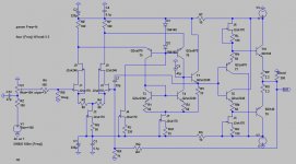

Earlier in this thread it was suggested that the voltage over the CM was too small. The CE voltage with no extra diodes is 620 mV. Do you think this is enough?
Sure--these parts will saturate somewhere at 200 mV, so we're a long way from that. Operating BJTs at 0 V base-collector voltage is no problem at all (see e.g. Q5/Q6 in the AD797 schematic)--sometimes it is thought that in this condition they're saturated already which is not true. Without R5 the collector voltage would be on the low side though as noted before.
The key point is that R5 introduces the very right voltage drop to operate T3/T4 at the same collector voltage because R5 = 0.5 * R1 and Ic (T3) = 0.5 * Ic (T1). If you add a diode then the voltage is too high again, a temperature coefficient is introduced and voltage swing reduced. You could rebalance things by adding a single (not two) diode between T3 C-B but there's no advantage compared to the simpler no-diode case.
The latest revision looks fine to me except that I'd probably add the 47 pF distortion cancellation cap from output to T5 collector.
Samuel
Last edited:
R1/R2 = 78 mV and R5 = 87 mVWhat's the DC across R1, R2 and R5 with no input signal?
Samuel
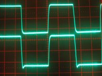
I don't know why I get this dip. It doesn't show up like this in LTSpice. The square looks like this in sim if T1 is "starved" for current.
I think the effect is related to C7. On fast negative edges this capacitor draws current from T1. Possible solutions include:
* Reducing C7 in value to the extent that stability is maintained.
* Use of a speedup-cap from output to J7 source which dynamically increases the collector current of T1; a couple of pF should be enough.
* Reconnecting C7 to T6 collector or distributing the capacitance between T6 collector and T1 emitter (e.g. 10 pF each).
On the other hand I'd say that a 100 kHz full-power square wave is a poor approximation to audio signals. I presume this is a dynamic effect which happens under large-signal/slew-rate conditions only. Very unlikely that any audio signal will ever trigger such. But of course if any of the above means work I'd fix it too.
Samuel
I'll try some of these suggestions.I think the effect is related to C7. On fast negative edges this capacitor draws current from T1. Possible solutions include:
* Reducing C7 in value to the extent that stability is maintained.
* Use of a speedup-cap from output to J7 source which dynamically increases the collector current of T1; a couple of pF should be enough.
* Reconnecting C7 to T6 collector or distributing the capacitance between T6 collector and T1 emitter (e.g. 10 pF each).
On the other hand I'd say that a 100 kHz full-power square wave is a poor approximation to audio signals. I presume this is a dynamic effect which happens under large-signal/slew-rate conditions only. Very unlikely that any audio signal will ever trigger such. But of course if any of the above means work I'd fix it too.
Samuel
You're right. It only happens under the conditions you mention. The test was done with the supply from 8 AAA's. It's not visible at higher supply or at lower signal.
I've started to '797-ize one of my other amps. I've finnished 1 channel so there are 2 more to go. This one did sound very good before the mod. I hope it improves in the same way as the JFET input amps did. I'll report back when I'm done. I need some more small caps to finnish it, so it'll take a couple of days.
The different input stages sounds different, and I think the difference is more obvious after '797-izing the amps.
Standard JFET: neutral to warm, typically JFET grainy and aggressive, improved a great deal after being '797-ized - not as "tubby" and a lot cleaner
JFET/JFET cascode: brighter than the above, more details like reverbation/room information, less grainy, maybe a bit "hard", also improved after '797-izing but has become a bit on the lean side
JFET/bipolar CFP: unchanged tonality compared to standard JFET but cleaner, less tubby, simply better, I don't think I can convert it to '797-style because it's a bit messy, but I'll probably give it a try
bipolar/bipolar CFP: very warm, sweet and smooth, details still on par with the more aggressive JFET amps but not as neutral in tonality and not the same accuracy in soundstage (where JFET amps usually excell in my oppinion), about to be '797-ized
Regarding bipolar transistors, it was totally uninspiring from start when I used BC549/559 from NXP. With SA970/SC2240 it was too bright and "flat". SA1016/SC2362 made all the difference.
Attachments
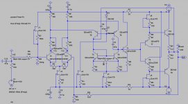
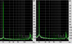
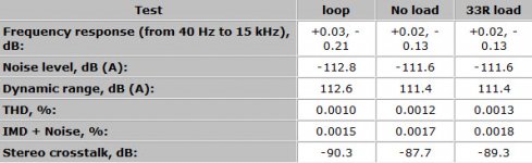
The amp with bipolar CFP input stage turned out to sound really beatiful. Warm and detailed. Smooth and laid back compared to the JFET input amps. Again it's the details such as room information/reverb effects that improved, and everything sounds cleaner. It measures well in RMAA and looks OK on the scope.
Left fft is E-mu 1212M loop-back and right is this amp with 33R load. On the scope it's 100 kHz, 1V, 33R load.
Left fft is E-mu 1212M loop-back and right is this amp with 33R load. On the scope it's 100 kHz, 1V, 33R load.
Attachments

- Status
- Not open for further replies.
- Home
- Amplifiers
- Solid State
- Discrete AD797 up and running