According to datasheet writes to 0xF000 - 0xF002 and 0xF005 take effect only after PLL is enabled (0x01 to 0xF003). So you should read those registers after PLL is enabled.
Code:
F890: 00 00
F890: 00 01
F400: 00 00
F400: 00 01
F403: 00 00
F403: 00 01
F003: 00 00
F000: 00 60
F001: 00 00
F002: 00 00
F005: 00 00
F003: 00 01
F050: 1D 33
F051: 00 00
F024: 01 40
F025: 00 31
F422: 00 00
F450: 00 01
F514: 00 06
F797: 00 00
F100: 00 01
F101: 00 08
F102: 00 10
F103: 00 18
F104: 00 20
F105: 00 28
F106: 00 30
F107: 00 38
F140: 00 06
F180: 00 03
F181: 00 03
F182: 00 02
F183: 00 02
F184: 00 02
F185: 00 02
F186: 00 02
F187: 00 02
F188: 00 02
F189: 00 02
F18A: 00 02
F18B: 00 02
F18C: 00 02
F18D: 00 02
F18E: 00 02
F18F: 00 02
F190: 00 02
F191: 00 02
F192: 00 02
F193: 00 02
F194: 00 02
F195: 00 02
F196: 00 02
F197: 00 02
F200: 00 40
F201: 00 22
F204: 90 00
F205: 00 22
F208: 90 40
F209: 00 22
F20C: 90 00
F20D: 00 22
F210: 90 40
F214: 90 00
F218: 90 00
F21C: 90 00
C000: 00 00
0000: 00 00
6000: 00 00
F403: 00 00
F404: 00 00
F401: 00 02
F402: 00 00
F402: 00 01
F400: 00 00
0xF428 Panic code: 00 02
0xF002 PLL enabled: 00 00
0xF004 PLL lock: 00 01

[ATTACH=full]1472980[/ATTACH]
Seems got lock but panic code is 2, probably some misconfiguration is asrc?
If uncomment printing of i2c read got lock + panic code 1
Code:
0xF428 Panic code: 00 01
0xF002 PLL enabled: 00 00
0xF004 PLL lock: 00 01
Actual working function. The rest of things in original unmodified generated C code from sigma studio, no need to make special order!
Code:
void SIGMA_WRITE_REGISTER_BLOCK(uint8_t addr, uint16_t regAddr, uint16_t length, uint8_t *value)
{
	HAL_StatusTypeDef status;
	uint8_t timeout = 0;
	uint8_t rr[2], ff[2+length];

	rr[0] = (regAddr >> 8) & 0xff;
	rr[1] = regAddr & 0xff;
	ff[0] = rr[0];
	ff[1] = rr[1];
	memcpy(ff+2, value, length);

	while(1)
	{
		status = HAL_I2C_IsDeviceReady(&hi2c1, addr, 3, 500);

		if (HAL_BUSY == status)
		{
			// 1.5 seccond timeout
			if (timeout == 3)
			{
				Error_Handler();
				return;
			}

			timeout++;
			continue;
		}

		if (HAL_ERROR == status || HAL_TIMEOUT == status)
		{
			Error_Handler();
			return;
		}

		if (HAL_OK == status)
		{
			if (HAL_OK != HAL_I2C_Master_Transmit(&hi2c1, addr, ff, length+2, 4000))
			{
				Error_Handler();
				return;
			}
#if 0
			char bufercic[64];
			extern void UART_TX(char *ch, uint16_t sz);
			HAL_StatusTypeDef status;

			uint8_t nn[2];
			nn[0] = rr[0];
			nn[1] = rr[1];

			status = HAL_I2C_Master_Transmit(&hi2c1, 0x70, nn, 2, 500);
			if (HAL_OK == status)
			{
				status = HAL_I2C_Master_Receive(&hi2c1, 0x71, nn, 2, 500);
				if (HAL_OK == status)
				{
					snprintf(bufercic, 64, "%02X%02X: %02X %02X\r\n", rr[0], rr[1], nn[0], nn[1]);
					UART_TX(bufercic, strlen(bufercic));
				}
				else
				{
					snprintf(bufercic, 64, "error2!\r\n");
					UART_TX(bufercic, strlen(bufercic));
				}
			}
			else
			{
				snprintf(bufercic, 64, "error!\r\n");
				UART_TX(bufercic, strlen(bufercic));
			}
#endif
		}
		else
		{
			Error_Handler();
			return;
		}

		break;
    }
}Final check
I'm still having panic=2 but printed zero as a masked out panic for asrc0 and asrc1, need to fix configuration in sigma studio
Code:
0xF004 PLL_LOCK: 00 01
0xF002 PLL_CLK_SRC: 00 00
0xF026 CLK_GEN3_SRC: 00 0E
0xF021 CLK_GEN1_N: 00 01
0xF020 CLK_GEN1_M: 00 06
0xF023 CLK_GEN2_N: 00 01
0xF022 CLK_GEN2_M: 00 09
0xF025 CLK_GEN3_N: 00 31
0xF024 CLK_GEN3_M: 01 40
0xF000 PLL_CTRL0: 00 60
0xF001 PLL_CTRL1: 00 02
0xF003 PLL_ENABLE: 00 01
0xF005 MCLK_OUT: 00 01
0xF006 PLL_WATCHDOG: 00 01
0xF401 START_PULSE: 00 02
0xF428 Panic code: 00 00
I'm still having panic=2 but printed zero as a masked out panic for asrc0 and asrc1, need to fix configuration in sigma studio
Last edited:
Got pulses, hmm but lrck is 2kHz and bck is 128kHz, might be that missing some clock configuration
Sadly but serious isues happened in relation to i2c read on all 2 comtrue pcm2dsd, dsd2pcm, everything was wrong because of misread to i2c devices and wrong values write to registers trought unsucesfull read, that put H bridge into PCM768 mode, also status mute pin was wrong, this misconfiguration killed H bridge and probably last time that killed all 3 comtrue! Now everything is correct but H bridge is dead and I will need to order new gates : (
bohrok2610 was right in relation to HAL i2c read, addr+1 is wrong! Thats in most case isue on my seccond diy device.
For example:
ReadReg always read 0 and after bit correction the whole things which uses similar pieces of code doing the same wrong value write, that was fatal sw bug
bohrok2610 was right in relation to HAL i2c read, addr+1 is wrong! Thats in most case isue on my seccond diy device.
For example:
Code:
	tt = CT7302_ReadReg(CT7302_DSD_ADDRESS, 0x49);
	tt &= ~(1 << 3);
	CT7302_WriteReg(CT7302_DSD_ADDRESS, 0x49, tt);
Last edited:
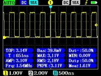
CT7302 have problem with register 0x16, for example when no track at i2s input than mute status out pin need to be low but its high! That killed H bridge because complementary gate on i2s input highly depend on this mute status pin from CT. Register 0x16 from CT have default value 0x56 which is in binary form 01010110, I have tried to put 0x55 which is 01010101 but it not fixed mute status out pin, its always high but need to be low when no track at i2s input. Looking into picture on dsd64 I found that freq is wrong, 1.54MHz which is half of the 48k x 64, so this from picture might tell that patern on picture is 00110011 so silence patern for mute in register 0x16 need to be 0x33! I will try! When those status pin gets fixed than I will order new gates for H bridge othervise no go further, dead end.
Attachments
Last edited:
- Home
- Amplifiers
- Class D
- Direct Digital Power DAC (DDPD)