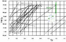
The dynamic resistance is inversely proportional to the bias current. basically, as voltage is a logarithmic function of current (ignoring capacitance) and differentiating a log gives a reciprocal.
All the above are true, so none of the above is useful.
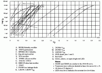
Bob Pease had some actual measurements and associated thoughts. But he was so prolific they are hard to find. This (below) is preserved in the back of his book.
IIRC: on LOG plot a basic diode is "linear" (really loggy) above leakage and below parasitic resistance. Series resistance on modern parts is small until you get to the last decade of rated current.
And "dynamic resistance" follows Shockley's Law over many decades of current.
There is no useful "threshold". It may look that way on a linear plot but on log plot it is the same curve all the way down (to leakage).
BUT "computer" diodes (most of our basic diodes) are Gold-Doped which bends their curves.
If you want log-curve a buffered BJT is the usual best-fit.
If you want a "threshold" you want an amplified diode and reference voltage.
Attachments
Sigh..
A power diode will never exhibit 2.2 mV /degree C. Most run in the .9 to 1.5 mV/C. This is a consequence of running the device in the large injection regime. I have verified this for diodes from 1 amp out to 7000 amps over the years.
In the mid 80's I worked for a diode manufacturer, and noted every manufacturer out there tested tempco incorrectly, so provided bad data sheet information.
Gold and platinum are used in the diffusion process to create lattice defects, those defects are used as recombination sites to absorb carriers, speeding up reverse recovery for high speed diodes. Gold unfortunately also increases reverse leakage as the temperature rises, so can cause thermal runaway in sims applications. Platinum is less dangerous in that regard.
Various diffusion profiles change the vf characteristic, as does the base wafer doping. Also, epitaxial devices can also be fast (hence the term Fast epitaxial rectifier, or "FER".
The base width of the junction is also important, as it can be designed in from zero to large. Zero base width makes a diode more radiation resistant, something I have to worry about.
Ah, almost forgot... I ran a 3 inch diameter diode at 100mA, 1 amp, 10, 100, and 1000 amps, the forward voltage stuck to the 60 mV per decade rule like glue.
Jn
Edit... a transistor E-B junction can track tempco at very close to the ideal 2.2mV/C.
Ps. Unfortunately, my copy of Sze is at work, otherwise I would specify pages. Also, my copy of Grove as well.
Last edited:
Sorry, have been away. My application is as a cathode 'resistance' over a range of 0.5 to 3mA. I want a constant 1.2V voltage (like 2 diode drops, but not critical) but a very low dynamic impedance (critical).
Jan
Jan
If you just stack two diodes, you get a differential resistance that's inversely proportional to the current. There is not much you can do about that, you can only try to keep the differential resistance low by using diodes with a low emission coefficient, that is, using the ones that have a steep curve in PRR's plot. The best you can get at room temperature is about 104 ohm at 0.5 mA, 17.3 ohm at 3 mA. If that's not good enough, use a different type of shunt regulator than two stacked diodes. The simplest alternative I can come up with is two diodes (or one LED) that conduct the cathode current plus some extra bias current that's >> 3 mA.
Last edited:
That is a great idea Marcel - that will decrease the current modulation and thus the impedance variation.
I will try that!
Jan
I will try that!
Jan
So if I take 2 diodes 1N4148 in series with a nominal current of 1.5mA, and vary the current +/-0.5mA, that will give delta-V of 64mV (Zd = 64 ohms), but when I pre-bias them with 7.5mA, the voltage variation is only 16.5mV (Zd = 16.5 ohms).
Using a diode-connected transistor should make it even better.
Jan
Using a diode-connected transistor should make it even better.
Jan
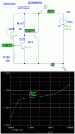
You could also try something like this, where 1 is the input node and 0 ground:
Q1 1 1 3 NPN
R1 3 0 150
Q2 1 3 0 NPN
That's a diode-connected Darlington with an extra resistor to bias the first transistor at a more or less constant current.
Q1 1 1 3 NPN
R1 3 0 150
Q2 1 3 0 NPN
That's a diode-connected Darlington with an extra resistor to bias the first transistor at a more or less constant current.
...a cathode 'resistance' over a range of 0.5 to 3mA. I want a constant 1.2V voltage...
NiCad cell.
That requires 120 C to reach 1.2 V, for example 12000 s at 10 mA. By that time the cathode is probably damaged.
Make one of then a 1N5819 and increase the bias current to 50mA.
I don't have 50mA to spare, maybe 5mA.
Jan
That requires 120 C to reach 1.2 V, for example 12000 s at 10 mA. By that time the cathode is probably damaged.
Worse, I may be dead by then ;-)
Jan
You could also try something like this, where 1 is the input node and 0 ground:
Q1 1 1 3 NPN
R1 3 0 150
Q2 1 3 0 NPN
That's a diode-connected Darlington with an extra resistor to bias the first transistor at a more or less constant current.
That drops the Zd from 16.5 to to 6 ohms. And it holds up at higher frequencies. Nice
Jan
R1 may need to increase if you have only 5 mA to spare. With R1 = 150 ohm the circuit only just starts to work at 4 mA or 5 mA.
With more components and setting the minimum current to about 1 mA:
Q1 2 3 1 PNP
Q2 3 3 0 NPN
Q3 1 2 0 NPN ;; preferably a type with high hFE
R1 1 3 1500
R2 2 0 1500
C1 1 0 1E-9 ;; or whatever is necessary to get rid of ringing
Q1 and Q2 set the voltage and run at more or less constant currents, Q3 takes care of the current variations.
This is Marcel's circuit, right? That seems very good. In fact it starts to look like those ic shunt regulators ...
Brain fart: how about a 3-terminal voltage regulator that could sink current? Hmmm.
Or maybe I should just stop while I'm ahead ;-)
Jan
Brain fart: how about a 3-terminal voltage regulator that could sink current? Hmmm.
Or maybe I should just stop while I'm ahead ;-)
Jan
It's similar, but not equal. It's my circuit from post #36 upside down, with reversed polarities of the transistors that are not diode connected, resistors redimensioned and compensation capacitor removed. I think you need to check the step response (or some other stability measure) to see if you can do without the compensation capacitor.
- Home
- Design & Build
- Parts
- Diode physics