I want to make a switcher for digital audio signals (S/PDIF) that I can control from an Arduino.
I happen to have a stand-alone digital audio switcher so I thought I'd trace out that schematic and see how it works.
I'd appreciate some help understanding how this circuit works and why it is done this way?
The majority of this is pretty simple, the input obviously goes to a 74HC4052 (two of them, because this switches two independent outputs) which are high bandwidth analog switches. After switching the signal is fed to a 74HC04D which is a Hex inverter. Am I correct thinking this is simply to buffer the output?
The main bit I don't understand is why they have this resistor divider around the hex inverter. I can see they are chaining two sets of input/outputs in series to get back the 'non-inverted' signal, but why the resistors?? Can someone help here?
Thanks!
My best guess is the upper of the two 10k resistors is being used to bias the HC04 to operate as a linear amplifier. Its a bit low in value for that though. The lower one I have no idea what its purpose is. To use a logic gate as linear amp normally is done with the HCU04, not the HC04 though - the 'U' standing for 'unbuffered' so it draws less quiescent current in linear mode.
Does the 75HC04D amplify the signal in default operation? I note in the datasheet at 4.5V VCC it accepts In logic high 2.5V but output logic high is 4.5V.
I think they are basically taking half the original signal and subtracting it from the output of the first stage (which is inverted phase), in order to reduce the level feeding the second stage.
But why not just use a standard voltage diver on the output of the 1st stage rather than use phase cancellation?
Last edited:
It's very sloppy that they left pins 5 and 9 floating, by the way. I also miss the input termination resistors. Then again, maybe the schematic is simply incomplete.
Like abraxalito already wrote, the first inverter is used as an analogue amplifier (biased by the 10 kohm shunt feedback resistor), the second turns the amplified signal into rail-to-rail square waves. I can only guess what the 10 kohm resistors to ground are meant for; maybe to create a small offset so the second inverter goes to a fixed and predictable level when there is no input signal? Then again, that offset will be very small with a 74HC04, it would work much better with a 74HCU04.
When used as a feedback amplifier, a 74HC04 is more prone to oscillations than a 74HCU04. Maybe the S/PDIF input drives the first inverter hard enough to keep it from oscillating? But then what happens when the input is open or the S/PDIF source is switched off? Or is there simply a typo in the part number on the schematic?
Last edited:
Hi,
It's all optical I/O.
I drew the schematic and missed out bits that didn't seem important like grounded unused pins.
I'm not familiar with logic ICs. I thought the hex inverter created rail to rail output so long as the input was within the detection threshold? I guess I must be wrong.
If I were right I don't understand how negative feedback changes the output level.
Another Q - Since the output is optical, I'm not entirely sure a buffer is necessary? Is it just because the CMOS switch is not very linear unless it feeds a high impedance? Or the optical RX can not drive the TX without a buffer?
Sorry for my noob questions, like I said I usually do analog audio so never really worked with logic level stuff before.
Last edited:
An unbuffered inverter is just an NMOS common source stage and a PMOS common source stage that are essentially in parallel, as in the attached picture (details such as ESD protection left out for clarity). When you drive it with full-swing or nearly full-swing signals, the transistors are switched on and off completely and the whole thing works as an inverter. For small signals around the point that makes the output go halfway between supply and ground, it is just an amplifying stage - like I wrote, two common source stages in parallel.
A buffered inverter is three unbuffered inverters in a row. Since you are used to analogue electronics, you probably understand that a negative feedback loop around a single pair of paralleled common-source stages is easier to keep stable than a loop around three such stages. With three stages, you have more loop gain and more phase shift in the loop, so it gets more difficult to comply with Nyquist's or Bode's stability criteria.
A buffered inverter is three unbuffered inverters in a row. Since you are used to analogue electronics, you probably understand that a negative feedback loop around a single pair of paralleled common-source stages is easier to keep stable than a loop around three such stages. With three stages, you have more loop gain and more phase shift in the loop, so it gets more difficult to comply with Nyquist's or Bode's stability criteria.
Attachments

Thank you for the detail!!
What is the purpose of 74HC04 in this circuit? Why not simply connect the optical RX to the TX through the CMOS switch? 😱
What is the purpose of 74HC04 in this circuit? Why not simply connect the optical RX to the TX through the CMOS switch? 😱
Good question, I haven't a clue. Using typical optical receivers with CMOS-level outputs and typical optical transmitters with CMOS level inputs, the multiplexers by themselves should suffice. I also don't see the point in using AC coupling then.
Are there variants on the market that have coaxial S/PDIF inputs and outputs? If so, then maybe the manufacturer tried to design one PCB that can be used with optical and coaxial inputs and outputs. For coaxial you would need a voltage divider after the 74HC04, but maybe they reserved board space for that?
Are there variants on the market that have coaxial S/PDIF inputs and outputs? If so, then maybe the manufacturer tried to design one PCB that can be used with optical and coaxial inputs and outputs. For coaxial you would need a voltage divider after the 74HC04, but maybe they reserved board space for that?
I don't see space for a voltage divider on the output.
Another couple of noob questions if you don't mind -
Why bias the gate? If the reason is to get reduction in gain on the 1st section, is this method somehow better than just add a voltage divider on the output of the 1st gate?
Why do they use a hex inverter? Why not use a non-inverting buffer?
Thanks for the education!
I don't know why they use AC coupling and buffering at all, but suppose you were to make a similar circuit with coaxial S/PDIF inputs. A coaxial S/PDIF input has to be terminated with a 75 ohm resistor to prevent transmission line reflections, it has essentially no DC bias (< 50 mV) and the level on an S/PDIF line is nominally 0.5 V peak to peak, but receivers are required to work reliably with anything from 0.2 V to 0.6 V peak to peak (as prescribed in chapter 7 of the standard IEC60958-1).
A normal CMOS gate is only guaranteed to interpret anything below 30 % of the supply voltage as a low level and anything above 70 % as a high level. The voltage range in which it transitions from low to high is normally quite narrow, but where this range is located in voltage depends on things like process variations and temperature.
Suppose you would somehow shift up the S/PDIF signal voltage by 2.5 V and apply it to a CMOS buffer running at 5 V supply. Its input signal would then switch between 2.4 V and 2.6 V for a weak and between 2.2 V and 2.8 V for a strong S/PDIF signal. As all these values are between 30 % and 70 % of the supply voltage, the output of the buffer could then be continuously low, continuously high or have the desired signal on it, depending on process variations and temperature.
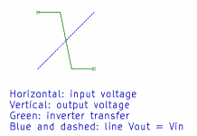
Using AC coupling and a feedback resistor across an inverter, the inverter automatically biases itself somewhere around the centre of the transition range (which is also known as the trip level), provided it doesn't oscillate. You will see that it has to bias itself like that when you look at the drawing. The feedback resistor forces the input DC voltage to equal the output DC voltage (dashed blue line), but they also have to be on the green curve that shows the relation between inverter output and input voltage. You need an inverter, because with a buffer, the green curve would be reversed and the input and output voltages would either both become 0 or both become equal to the supply voltage. (Theoretically it could also end up on the correct bias point, but a more complete analysis shows that the correct bias point is unstable when you use a buffer - you get positive feedback instead of negative feedback.)
When the inverter is biased at its trip point, an input signal of a few hundreds of millivolts is probably sufficient to make its output switch reliably, again assuming the feedback doesn't make it oscillate. Even when the signal is too small to make the first inverter switch, it amplifies the signal and makes the second inverter switch (inverters in the same hex inverter chip match, so their trip levels will be quite close).
A normal CMOS gate is only guaranteed to interpret anything below 30 % of the supply voltage as a low level and anything above 70 % as a high level. The voltage range in which it transitions from low to high is normally quite narrow, but where this range is located in voltage depends on things like process variations and temperature.
Suppose you would somehow shift up the S/PDIF signal voltage by 2.5 V and apply it to a CMOS buffer running at 5 V supply. Its input signal would then switch between 2.4 V and 2.6 V for a weak and between 2.2 V and 2.8 V for a strong S/PDIF signal. As all these values are between 30 % and 70 % of the supply voltage, the output of the buffer could then be continuously low, continuously high or have the desired signal on it, depending on process variations and temperature.
Using AC coupling and a feedback resistor across an inverter, the inverter automatically biases itself somewhere around the centre of the transition range (which is also known as the trip level), provided it doesn't oscillate. You will see that it has to bias itself like that when you look at the drawing. The feedback resistor forces the input DC voltage to equal the output DC voltage (dashed blue line), but they also have to be on the green curve that shows the relation between inverter output and input voltage. You need an inverter, because with a buffer, the green curve would be reversed and the input and output voltages would either both become 0 or both become equal to the supply voltage. (Theoretically it could also end up on the correct bias point, but a more complete analysis shows that the correct bias point is unstable when you use a buffer - you get positive feedback instead of negative feedback.)
When the inverter is biased at its trip point, an input signal of a few hundreds of millivolts is probably sufficient to make its output switch reliably, again assuming the feedback doesn't make it oscillate. Even when the signal is too small to make the first inverter switch, it amplifies the signal and makes the second inverter switch (inverters in the same hex inverter chip match, so their trip levels will be quite close).
Attachments
Last edited:
Using AC coupling and a feedback resistor across an inverter, the inverter automatically biases itself somewhere around the centre of the transition range (which is also known as the trip level), provided it doesn't oscillate. You will see that it has to bias itself like that when you look at the drawing. The feedback resistor forces the input DC voltage to equal the output DC voltage (dashed blue line), but they also have to be on the green curve that shows the relation between inverter output and input voltage. You need an inverter, because with a buffer, the green curve would be reversed and the input and output voltages would either both become 0 or both become equal to the supply voltage. (Theoretically it could also end up on the correct bias point, but a more complete analysis shows that the correct bias point is unstable when you use a buffer - you get positive feedback instead of negative feedback.)
When the inverter is biased at its trip point, an input signal of a few hundreds of millivolts is probably sufficient to make its output switch reliably, again assuming the feedback doesn't make it oscillate. Even when the signal is too small to make the first inverter switch, it amplifies the signal and makes the second inverter switch (inverters in the same hex inverter chip match, so their trip levels will be quite close).
Okay this is a great explanation, thanks so much!
I'm still rather unclear about the difference of the buffered or unbuffered hex inverter. Will the 'U' variant still be able to provide a high impedance input and low impedance output?
Last edited:
A 74HCU04 inverter certainly provides a high-impedance input. When the input is driven hard enough to turn its MOSFETs completely on and off, it has a similar output impedance as any normal 74HC logic gate. When you use it as an analogue amplifier, the output impedance is much higher than when you switch it completely.
Suppose you would use 74HCU inverters in a circuit like you posted. There is always an inverter connected as an analogue amplifier followed by a second inverter. The first one may have a highish output impedance, but as long as the swing at its output goes from close to ground to close to VDD, the second inverter is driven pretty hard and has the usual 74HC* series output impedance.
Practically, the main difference between a 74HC04 inverter and a 74HCU04 inverter is that a 74HC04 inverter has a higher voltage gain around its trip point because it internally consists of three inverters in a row rather than a single one, and a 74HCU04 is much less prone to oscillations when used as an analogue amplifier because it internally consists of a single inverter rather than three in a row.
Last edited:
Okay I'm building the schematic for my own design. I'd like to ask - I have two 3.3V lines, one for analog (running my DACs too) and one for digital including the micro controller.
Would you run the MUX 74HC4052 for SPDIF on the analog or digital line?
Would you run the MUX 74HC4052 for SPDIF on the analog or digital line?
Digital, as I would expect crosstalk from the S/PDIF signals to the analogue part of the DAC to have more impact on the performance than crosstalk from the microcontroller to the S/PDIF signals. This is only based on gut feeling, though.
- Home
- Source & Line
- Digital Line Level
- Digital Audio Switcher MUX