What's the major differences between those single transistor based,darlington based,complementary or FET??Any link or guide??
Hi,
A bias using a Sziklai complementary pair is described by Douglas Self in the fourth edition of his "Audio power amplifier design book" pages 378-379. Compared with a single transistor, the dynamic impedance is lowered more than ten times.
One of the first high power amplifiers using it was the Revox A740, schematics is here, page 30 :
ftp://ftp.studer.ch/Public/Products/Revox/Revox_A740/Revox_A740_Serv.pdf
Also described in one of the first issues of the french magazine "l'Audiophile"
I see interesting things about VBE multiplier in simulator. The VC-E is following the signal, not a stiff steady voltage like I used to think. And the VC-E is all used when the output stage is swinging heavy on 1 side (the other inactive side got no/little bias).
My question was more specifically pointed on a single complementary NPN/PNP (Non CFP/Siklai) vs. a single BJT, or eventually the "double complementary CFP (NPN/PNP -PNP/NPN) vs. a single CFP (NPN/PNP).
I mean the ressistor between the bases define the current, then the resistors between bases and collectors the voltage.
I mean the ressistor between the bases define the current, then the resistors between bases and collectors the voltage.
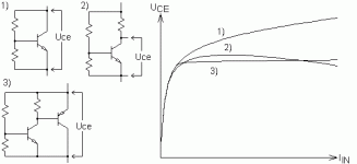
The inclusion of the "current-compensation" resistor (in single-transistor circuit) causes VCE to decrease when the input current increases. With the choice of resistor value the steepness of VCE limiting can be controlled. In essence, the value of should be optimized so that only slight voltage variations occur around the optimal bias voltage setting.
With the addition of another transistor (usually in the form of Sziklai pair) the loop gain of the VBE multiplier circuit can be increased. The first transistor serves as the temperature sensor while the second transistor amplifies its effect. The technique can reduce the resistance slope (U versus I) of the multiplier but substantial results are gained (again) only after the inclusion of current-compensation resistor. The advantages are a high linearity regardless of input current and a broader tolerance for values of current compensation resistor.
The results of using various configurations follow approximately the curves shown in the attachment. The linear the curve is, the better. The Sziklai pair can provide very linear performance but unfortunately it is extremely unstable. Using Miller capacitance can compensate the poor behaviour somehow but this is just a band-aid.
I don’t like the 2-transistor configuration because any instability in bias servo can have dreadful consequences. The single-transistor with current compensation works well although its behaviour depends a lot on device parameters such as beta.
I don’t know about FETs and MOSFETs but I remember something along the lines that they are used with MOSFET output transistors because of their somewhat better parameter matching with those than what the ordinary BJTs have. I could be wrong, though.
Attachments
re post9 diagrams.
I like the D. Self extra resistor version.
The resistor value moves the peak (graph 2) to alternative currents and can be used to obtain near linearity at the actual operational VAS current.
Another resistor in the emitter leg reduces the temp compensation slope.
I wonder if that is what the LED in the Sony does as well?
Topology for Great Risc for Fire-Up of the Power Darlington Buffer Stage
The topology of fig. 2d is the best solution, but the version of fig. 2b (mostly to find) about
http://peufeu.free.fr/audio/articles/Vbe Multiplier.pdf
exist in four subvariants.
The last both from attachement are not recommend, because in case of an internal interrrupt by the variable resistor the maximum possible idle current flows from the power supply. Nevertheless this topologies are often to find. Bat what could therefore the reason?
And is there an advantage resp. special characteristic between the first both variants?
Attachments
2d in Hagerman is D.Self with extra resistor and the replacement of the upper resistor with a diode connected transistor.
I'll stick with the D.Self + extra resistor. It's simple. It works. Post9 fig 2)
I'll stick with the D.Self + extra resistor. It's simple. It works. Post9 fig 2)
Last edited:
Maybe the brightness of the LED is an indicator for the voltage value between C and E and thus an Indicator for the idle current through the output power devices.Hi all.
What is the purpose of the led in the Vbe Sony. Why?
Geirin
NAD's Vbe solution from the integrated amplifier model 306 looks interesting (for me very special) - go to the attachement from post #1 about
http://www.diyaudio.com/forums/soli...better-audio-non-complements-audio-power.html
(second schematic).
What is the justifying for this topology?
Last edited:
When using On-Semi ThermalTrak output transistors which include a thermal tracking diode, is there any advantage in putting the diode string within a Vbe multiplier circuit, or is it better to use only the diodes in series for thermal compensation in the bias circuit?
The Leach power amp puts the thermal tracking diodes between the collector and base of the Vbe multiplier circuit. Leach said that putting just the thermal diodes on the heatsink and leaving the Vbe transistor on the main PCB put the capacitance and inductance of any wires required to connect the thermal device in the least sensitive circuit path.
The Leach power amp puts the thermal tracking diodes between the collector and base of the Vbe multiplier circuit. Leach said that putting just the thermal diodes on the heatsink and leaving the Vbe transistor on the main PCB put the capacitance and inductance of any wires required to connect the thermal device in the least sensitive circuit path.
Last edited:
Please post the associated web addresses - thank you.There are a couple of threads discussing the ONsemi Thermal Track and on ways to bias them.
- Home
- Amplifiers
- Solid State
- Differences between various vbe multipliers