Hi,
I don't recall anyone ever talking about RMS power output since post #1. So, sailing right along with that convention, we can surely say it's a 900W amp, if the original half bridge was a 100W amp into an 8ohm load.
Regards,
Chris
I don't recall anyone ever talking about RMS power output since post #1. So, sailing right along with that convention, we can surely say it's a 900W amp, if the original half bridge was a 100W amp into an 8ohm load.
Regards,
Chris
Interesting tread i must say!
But there is still some minor things to deal with:
I know the importace of swithing fast, but the mosfets are kind of prone to oscillate without gate resistance.
There is some info given: the upper halves seem to bee hotter than lower, as i've read it in the tread.
The upper halve's swithing network have a power suply and its bias current that passes the lover halve output mosfets. so is not happening in the upper halve.
Deriver bias from current sorces may bee better.
The common mode is not fully dealt with, but can bee fedback in the switching networks or at the balanse of the switching from input stage..
There is more work to bee done...
Konrad,
Oscillation is only a problem when MOSFET’s are used in Linear mode (Class A/B etc) – and not when hard switched as in Class D. Gate resistors only increase switching losses, and have no place in a fast output stages – apart from maybe slowing Ton times.
The “heating” issue has been balanced by the use of Cascade level shifters.
The tiny extra “High Side” Driver current flowing thru the lower devices is insignificant compared to the switching losses / output current, and does not in reality cause a problem.
From what I see Chris and others have been working on, I'm looking forward to seeing the circuit - and hardware results
Cheers,
John
I don't recall anyone ever talking about RMS power output since post #1.
So, you’re reasonable for all those Mid-system Output Power ratings! 😉
John
JohnW said:
So, you’re reasonable for all those Mid-system Output Power ratings! 😉
John
Hi,
450W RMS more than meets my personal amp goal anyway. If we start talking RMS power now I dont' think anyone will want the half bridge version, which is 100 peak as well, someone should have spoken up about that long before now. Tell ya what I'm flexible... I'll call it a 450W RMS amp.
Konrad,
The comment I made awhile ago about the upper mosfet running hotter was with respect to a stripped down, plastic proto board version which I'd just made for kicks. Since it's not the way to make an amp like this.... I wouldn't project it's failings onto this design in any way, I also certainly would not attempt to produce my current circuit in the same poor fashion, at 450W RMS.. 😉 ..We need proper techniques even just for a prototype.
Regards,
Chris
Hi,
For all the hardcores who've been following this thread, you can find the full bridge circuit I've been working on here:
http://www.diyaudio.com/forums/showthread.php?s=&threadid=40307
Regards,
Chris
For all the hardcores who've been following this thread, you can find the full bridge circuit I've been working on here:
http://www.diyaudio.com/forums/showthread.php?s=&threadid=40307
Regards,
Chris
Here's the little prototype amp I made, as requested, half bridge UCD 15V rails.
It's quite the little performer, kind of noisy on a plastic protoboard but the characteristic of the audio shines through! Say's alot for it I think, considering. I think it would be worth making a PCB for.
The Tip127 is of course extreme overkill ... but I ran low on 2n3906's, so it got the job done. It could be optimised more I'm sure.. but I was more interested with playing it than playing with it.
Here's how this simulates:
1.2volts input @ 20khz ~43Watts peak
DC COMPONENT = 1.437437E-02
TOTAL HARMONIC DISTORTION = 1.009981E-01 PERCENT
___________________
1 volt input @ 20khz
DC COMPONENT = 1.203865E-02
TOTAL HARMONIC DISTORTION = 4.605130E-02 PERCENT
_________________
0.5 volt input @ 20Khz
DC COMPONENT = 1.174075E-02
TOTAL HARMONIC DISTORTION = 2.375277E-02 PERCENT
___________________
0.5Volts input @ 1Khz
DC COMPONENT = 1.128617E-02
TOTAL HARMONIC DISTORTION = 1.332616E-02 PERCENT
So yeah, have fun with it.
Chris
Attachments
Thanks for that.
So this is the softcore version.😀
I might just get my head round it. I'll try it in my simulator first.
Cheers
So this is the softcore version.😀
I might just get my head round it. I'll try it in my simulator first.
Cheers
Hi Johnnyx,
I'll give you some more info to help clarify things for you.
The zeners are 10 volt zeners, again, it's what I had around. The zener on the upper driver is required in order to pre-charge the bootstrap capacitor to ensure it can switch when you first power up the output stage.
The lower zener is required to match the upper and lower driver voltage supplies, since it's a 12 volt regulator used and not a 10 volt one. So you can simplify things there as well.
Now that I think about it.. I didn't need the 12 volt regulator at all, but the original mistake was using the 12 volt regulator and the 10 volt zener on the upper driver = smoked a few mosfets/speakers due to the unequal gate drive, that was a bandaid job, I should have torn out the 12V regulator while I was at it. Think I'll do that tonight.
Aside from that, it's bare bones as it can get, you'll get it.
Hi,
I see what you're going for and it's neat!
I have to ask though, does it really float? -V would tie to the source of the upper fet? With +V to the gate driver? If I'm not mistaken it looks like -V might be biased at some point between the power rails but not actually floating with the load, it's actually amplifying voltage /current to it.
Opto-couplers, when used for gate drivers, are there to isolate and level shift, you still require a seperate floating supply to power them with.
They also degrade over time.
What I propose for the upper floating supplies, since we need at least two of them, is to go with the ultra simple/low parts count way, put a few extra turns around the secondary of the main transformer, small full bridge.. few caps.. maybe build it up to 15 or 18 volts and slap a linear regulator on it of some type.
Should work good yes?
I'm not sure if the voltage stepping fuction of it would induce much noise into the other secondary's though.
Which I think is what you're trying hard to avoid if I'm not mistaken.
I pieced together a cheap & crappy class D amp from a TL074 quad opamp and two half-bridge IR2103 MOSFET drivers [full H bridge output]
I blew it up when I shorted the perf-board out while taking a measurement, and haven't touched in a few months. It's not great in the least, but if you guys want the schematic I'll draw it.
I blew it up when I shorted the perf-board out while taking a measurement, and haven't touched in a few months. It's not great in the least, but if you guys want the schematic I'll draw it.
raidfibre said:I pieced together a cheap & crappy class D amp from a TL074 quad opamp and two half-bridge IR2103 MOSFET drivers [full H bridge output]
I blew it up when I shorted the perf-board out while taking a measurement, and haven't touched in a few months. It's not great in the least, but if you guys want the schematic I'll draw it.
I say knock yourself out, I wouldn't mind seeing it 🙂 What type of modulation?
Sorry to hear about your smoke show! No doubt you've heard this already but just in case, it's a great idea to tape off all but the very tip of the meter leads just in case you twitch or slip it'll greatly reduce the odds of letting the smoke out.
classd4sure said:
It didn't work great, I blame my cheap implementation of it of course, it wouldn't play the full audio band, actually the mid range just died....highs and lows were ok, and it had a bit of a crackle at times. I also couldn't find a cap value low enough for the integrator, or had any testing equipment to try and tune it with.
Hi Chris,
Just join DIY today. First let me thank Johan and you for the help in exploring the unexplored territories of Class D.
About a year and a half back, I copied Johan's Class D amplifier schematic for my Project. Although it was a complete and a splendid design (richness of sound). i faced a lot of difficulty in getting it work (i blew 6 pair of costly MAX 626 driver
 )
)But , i was amazed to see the baby work!!
I am still a newbie in Class D design. I hope, i'll be enlightened on this amazing thing with your help.
Razor_Edge said:
Hi Chris,
Just join DIY today. First let me thank Johan and you for the help in exploring the unexplored territories of Class D.
About a year and a half back, I copied Johan's Class D amplifier schematic for my Project. Although it was a complete and a splendid design (richness of sound). i faced a lot of difficulty in getting it work (i blew 6 pair of costly MAX 626 driver
But , i was amazed to see the baby work!!
I am still a newbie in Class D design. I hope, i'll be enlightened on this amazing thing with your help.
Hello, welcome, and thank you.
I never attempted the all out version of it, just the basic idea with the bjt followers, veeery low power, on a cheap protoboard, ten minute wire job, this is why it didn't work well for me, but it made sound and that was a thrilling enough to make me want more.
I kept the air coil I made for it and used it in the UCD protoboard amp I wired, for what it is, it is a beast and I am most impressed with it, well worth the effort. It likes to burn mosfets every so often but hey.. protoboard. I was tempted to put it on PCB or at least wire it P2P, but I just lost an expensive soldering iron.
Regards
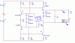
what's the two transistors on the left side used for? who can tell me?Konrad said:Talking abt driver and shot thru Here is a driver stage with a known delay on time and sims ok with nice switching.
Kenshin said:
what's the two transistors on the left side used for? who can tell me?
Hi. Q29 is the driver stage input. I think you are wondering why Q28 does not serve that purpose so that Q29, Q1, and Q19 can be eliminated. The main reason would involve timing of the MOSFET switching. Such good timing helps to lower distortion, reduce power dissipation in the MOSFETs, and lessen current spikes and associated noise when the MOSFETs switch.
I had thought of trying something with only the three transistors on the right, myself. It would be interesting to simulate both ways to see the differences.
subwo1 said:
Hi. Q29 is the driver stage input. I think you are wondering why Q28 does not serve that purpose so that Q29, Q1, and Q19 can be eliminated. The main reason would involve timing of the MOSFET switching. Such good timing helps to lower distortion, reduce power dissipation in the MOSFETs, and lessen current spikes and associated noise when the MOSFETs switch.
I had thought of trying something with only the three transistors on the right, myself. It would be interesting to simulate both ways to see the differences.
why not using a basic emitter follower and put all timing circuit at low side? A piece of logic chip can do all these things well,with fewer pins and more reliability.
- Status
- Not open for further replies.
- Home
- Amplifiers
- Class D
- Development of a "reference" class D starting point