which work well but have an ugly ring to them.
Maybe because they are "faster" than the other ones.
Regarding the driver circuits: It might be a good idea to test high- and low- side drivers seperately by using each output MOSFET "single ended", driving a resistor. So you are sure everything works O.K. before you close the loop (check timing with a scope). You could either drive the drivers themselves by a rectangular signal or drive the comparator input with a sinusoid (with the feedback removed).
To Ivan
I haven't tried it at 2.4 Volts input signal, but your figures look accurate. I never said that the circuit is optimised at all. I think some fine-trim of the comparator might help a lot. The transistors haven't been selected for best performance, they were just the models that I had within my trial version of P-SPICE. While the transistor models for the comparator might be quite O.K., the MOSFETs for the output stage definitely aren't. They are high current types with high gate-charge. You wouldn't use those for an amp with 35 volt rails, would you ?
And remember: You can always reduce the gain of the circuit by reducing the feedback resistor (and adjusting its parallel capacitor) and reduce THD at the same time.
I am still convinced that the general THD behaviour (i.e. THD vs frequency and THD vs input level) is the one favoured by many people.
Regards
Charles
Hi,
I wanted to post a few things but.....sigh.
If I click on pspice/generate netlist I get nothing like what you guys do. File/export doesn't give me a .sch option....how do you guys do it?
Chris
I wanted to post a few things but.....sigh.
If I click on pspice/generate netlist I get nothing like what you guys do. File/export doesn't give me a .sch option....how do you guys do it?
Chris
File/export doesn't give me a .sch option....how do you guys do it?
I simply take the .SCH file from the directory where PSPICE stores them and copy it.
Regards
Charles
whew.......almost lost it! Good thing for auto back up files I tell ya.
I thought of trying that....there isn't one. Would the .DSN file do the same trick?
Chris
I thought of trying that....there isn't one. Would the .DSN file do the same trick?
Chris
Hi, I finally stopped blabbing and produced something....good....bad.....you decide!
Note:
I spoke too darn soon regarding the quality of the BCXXX's, other factors were playing a roll..the 2n2222's have an ugly ring too with the IRF540's. In the end I stuck with em they work great, perhaps better. I also stuck with the IRF540's, better switching specs by far, but the strange thing is (and I dont' understand it), if you directly swap them for the IRF150's, they will have more cross conduction! Perhaps because of the lower RDS(ON)???
I Included several screenshots which I found interesting, one displays a "prime" reason for wanting class d in the first place, you'll know it when you see it!
Another I included shows an interesting if not worrysome relationship between the value of RB (lower comparator) and cross conduction of the output stage....hard to believe I know, given the anti saturation aspect of the driver stage.. but it's there and it's bad.
The file is too big so I'll split it up into two posts, that should do the trick nicely.
In the comming day's I'll attempt to modify it and add the second lead? network which Charles was nice enough to calculate.
I'm unable to tune it any better for a lower DC offset without sacrificing performance in the comparator output. Comments appreciated.
Regards,
Chris
Attachments
Hi. I suspect the main reason for the shoot through is that the IRF540 has a 360ns max diode reverse recovery figure while the one for the IRF150 is given as 500ns max.classd4sure said:
[SNIP]the IRF540's, better switching specs by far, but the strange thing is (and I dont' understand it), if you directly swap them for the IRF150's, they will have more cross conduction! Perhaps because of the lower RDS(ON)???
Chris
johanps said:I have now built the UCD circuit on a proto-board. Unfortunately, but not very surprisingly, I have not got it to oscillate by itself yet. (With the input connected to ground.)
This is because it is not "DC-stable" towards the positive rail. When I turn on my power supply, the comparator wants to make the output "high". But since the floating supply to the upper driver is made by a diode+capacitor, that driver can't hold the output high for very long. (Even though I have 22uF there now!)
For some reason then, it never manages to start oscillating. (Perhaps due to the way the voltages are ramped up.)
Once I got it oscillating by very briefly shorting the output to Vcc. Looked nice, but the second or third time I did it, I blew something 🙁
Thought I'd mention this, so you guys can help think about the DC-stability as well. (General DC/overload stability is likely to be a problem for most N-channel only designs (?))
/Johan
Hi Johan, the bootstrapped upper power supply needs to be refreshed by the lower mosfet turning on. It sounds like the comparator is trying to make the top mosfet turn on, but the lower one has not been on yet. It might be a good idea to figure on needing 12v/470ohm amperes (about 25ma or something) being constantly available to the upper mosfet driver. In experimental circuits I have built, I have derived the needed power from a floating winding on the USMPS output transformer.
subwo1 said:
Hi. I suspect the main reason for the shoot through is that the IRF540 has a 360ns max diode reverse recovery figure while the one for the IRF150 is given as 500ns max.
Hi. My brain is telling me the shorter reverse recovery would be better for cross conduction, I just woke up though and trust your judgment/experience, I'll have to look into that later so I better understand it.
Hi Johan, the bootstrapped upper power supply needs to be refreshed by the lower mosfet turning on. It sounds like the comparator is trying to make the top mosfet turn on, but the lower one has not been on yet. It might be a good idea to figure on needing 12v/470ohm amperes (about 25ma or something) being constantly available to the upper mosfet driver. In experimental circuits I have built, I have derived the needed power from a floating winding on the USMPS output transformer.
Well done, seriously, hats off. Same thing happens with the simulation too, upper switch wont' turn on until after the lower one does, so it always misses the first half of the wave.
Chris
subwo1 said:
Hi. I suspect the main reason for the shoot through is that the IRF540 has a 360ns max diode reverse recovery figure while the one for the IRF150 is given as 500ns max.
Ok I'm from what I understand the faster the recovery the better.
My data sheet shows Trr for the IRF540 as 170ns max, and yeah 500ns for the IRF150.
That's a noticeable difference which led me to believe I should see some improvement in shoot through with the IRF540.
I've simulated the mosfet currents extensively, it seems what the culprit here is what I've heard called "gate step" from high dv/dt which gets coupled to the gate via .....what I currently understand is a ratio between crss and ciss. Not exactly straight forward at all....looking for more information on it now anyway.
Step 1 to optimising is understanding the problem, can anyone recommend a good app note on this characteristic and don't say AN-6003 from fairchild because I have it on good authority it's highly flawed and should be disregarded.
Oh, on the lighter side of things, I also discovered spice doesnt' simulate this well at all due to poor modeling of ........well...here
"a step change in the gate voltage may be immediately seen
by perhaps 10% of the FET area, more after 5ns and more yet in another
5ns, with still more time required for 100% of the FET to see the gate-
voltage change. This is the realm of gate-spreading resistance, which
is very poorly modeled as a single lumped resistor." Win Hill
That said/quoted, leads me to believe that with this driver circuit in particular, I could almost go so far as to say shoot through may not actually exist in reality.
Can anyone actually confirm this? I think it would be good to clear this up given the nature of this project, people might shy away from trying it if they simulate and see kilo watt peak spikes over the switches, which is what is actually there, those low 1 watt dissipation graphs I posted are averaged...but if in reality they won't be there, the biggest fix required will be a few simple notes where the simulation greatly differs from reality.
Thanks,
Chris
Hi,
I think this information is of interest to anyone simulating or building the circuits previously posted with the ucd based driver circuit. It has to do with the sizing of the resistors in the gate drivers, timing of the signals, and shoot through.
I feel it solves the optimal condition for the timing of the drive signals, however shoot through will have to be cured elsewhere.
Regards,
Chris
Attachments
Shoot-through is mainly cured by correct timing. The terminology shoot-through is used for the current flowing because of two devices being simultaneously on.
But one will also encounter current-spikes due to the reverse-recovery of the MOSFET body diode.
One has to take care not to mix them up.
Regards
Charles
But one will also encounter current-spikes due to the reverse-recovery of the MOSFET body diode.
One has to take care not to mix them up.
Regards
Charles
phase_accurate said:Shoot-through is mainly cured by correct timing. The terminology shoot-through is used for the current flowing because of two devices being simultaneously on.
But one will also encounter current-spikes due to the reverse-recovery of the MOSFET body diode.
One has to take care not to mix them up.
Regards
Charles
Thanks for correcting my terminology.
In one of the screenshoots you clearly do see shoot through, the others are displaying dv/dt induced turn on, which I misstated as being "shoot through".
I dont' think it's from the body diode recovery time in this case.
The gate voltages there were taken across the turn off transistors in order to more clearly display the timing relationship, what they dont' show is the massive voltage spike on the gate causing the current spike, which you do see, and is of about 20 amps give or take.
So I guess that timing solution does in fact take care of any "shoot through" problem, but there's still a massive current spike which needs to be corrected somehow.
Hi,
Maybe it's not dv/dt either.
Would the body diode recovery only cause a turn off delay of the upper FET?
Maybe it's not dv/dt either.
Would the body diode recovery only cause a turn off delay of the upper FET?
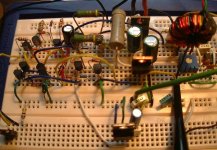
As I mentioned before, I have the circuit running on a protoboard now. I'm using BC546/BC556's, and 2 x IR640 instead of the corresponding components my the PSpice .sch.
See the attachment for a picture of my crummy implementation .
.
Thanks subwo1 - this is it! I added a resistor+13V zener pullup-circuit to the floating supply of the upper driver. This helps get the circuit going much more easily - but it's still not quite perfect. With this simplistic arrangement, the supply voltage needs to be about +/- 25V in order for the circuit to get going by itself...
But when it is going, it does produce sound that isn't displeasing to the ear at low to moderately high levels. (I'm using an old car-speaker to test with, and an sony walkman for the source.)
However, with this simple circuit, there is an issue with bias current to that comparator input, and DC-offset at the output. If I connect the source to the comparator input via a capacitor, the circuit refuses to oscillate at all (again not very surprising). So, for the early trial, I added a voltage-dividing bias supply to the input (two 12K resistors with a 20k pot. in between). With this I can adjust the DC offset at the output to near 0V - but a remaining problem is that the DC offset is not constant against the supply voltage.
I almost (mostly) agree. It can be discussed to which degree it meets all design goals, specifically regarding robustness - it has to start nicely when supplied with power in a suitable "recommended" voltage range. Also, when you do something wrong, and blow the circuit, one or more BJTs out of eleven may break together with one or both of the output mosfets. In this respect, IC's in sockets are much nicer 🙂
One more question that popped up in my mind is what the PSRR is? - Will this still work "good" when supplied by an unregulated power supply?
That said, I can't help thinking it's pretty cool that this circuit consisting of only discrete transistors works as good as it does. Hats off to Bruno again. 😎
So to conclude, if we want to use the UCD circuit more or less "as is" as the "reference starting point", we need to add some robustness, and address the DC offset issue. Tweaking component values and selection seems to be on-going
Anything else?
Ideas?
See the attachment for a picture of my crummy implementation
.subwo1 said:Hi Johan, the bootstrapped upper power supply needs to be refreshed by the lower mosfet turning on. It sounds like the comparator is trying to make the top mosfet turn on, but the lower one has not been on yet. It might be a good idea to figure on needing 12v/470ohm amperes (about 25ma or something) being constantly available to the upper mosfet driver. In experimental circuits I have built, I have derived the needed power from a floating winding on the USMPS output transformer.
Thanks subwo1 - this is it! I added a resistor+13V zener pullup-circuit to the floating supply of the upper driver. This helps get the circuit going much more easily - but it's still not quite perfect. With this simplistic arrangement, the supply voltage needs to be about +/- 25V in order for the circuit to get going by itself...
But when it is going, it does produce sound that isn't displeasing to the ear at low to moderately high levels. (I'm using an old car-speaker to test with, and an sony walkman for the source.)
However, with this simple circuit, there is an issue with bias current to that comparator input, and DC-offset at the output. If I connect the source to the comparator input via a capacitor, the circuit refuses to oscillate at all (again not very surprising). So, for the early trial, I added a voltage-dividing bias supply to the input (two 12K resistors with a 20k pot. in between). With this I can adjust the DC offset at the output to near 0V - but a remaining problem is that the DC offset is not constant against the supply voltage.
classd4sure said:It's too bad it turned out so close to the exact ucd patent, I was hoping to move away from it somewhat, but it's hard to beat it for simplicity, and it does meet all design goals, while remaining intuitive as to its operation.
I almost (mostly) agree. It can be discussed to which degree it meets all design goals, specifically regarding robustness - it has to start nicely when supplied with power in a suitable "recommended" voltage range. Also, when you do something wrong, and blow the circuit, one or more BJTs out of eleven may break together with one or both of the output mosfets. In this respect, IC's in sockets are much nicer 🙂
One more question that popped up in my mind is what the PSRR is? - Will this still work "good" when supplied by an unregulated power supply?
That said, I can't help thinking it's pretty cool that this circuit consisting of only discrete transistors works as good as it does. Hats off to Bruno again. 😎
So to conclude, if we want to use the UCD circuit more or less "as is" as the "reference starting point", we need to add some robustness, and address the DC offset issue. Tweaking component values and selection seems to be on-going
Anything else?
Ideas?
Attachments
Nice work.
I'm aware it still needs lots of work. My simulations showed adjusting DC offset being a real pain which is why I used a resistor instead of a current source in prior circuits, allowed for finer adjustment.
Still scratching my head over the drivers...
The idea I had for making it self starting was kicking it low on power up, but haven't thought about it enough to work out a solution.
Did you use equal driver resistors in your prototype?
Will you be posting the changes in spice as well?
Chris
Regarding the mosfet timing/shoot-through/ringing, I can offer the following observations from the protoboard implementation:
The switching-frequency is 330kHz. The output waveform (before the filter) looks very nice on the scope - perhaps just a hint of ringing after the output has transitioned from high to low.
Rise/fall times, as observed on the output, are about 100ns, or slightly better.
I do have problems with ringing on the lower gate; when the lower driver goes on, there's a spike, followed by a short pullback almost back to where it began, before the gate goes high for the rest of the half-cycle's duration. Then at the end, I can see the lower gate go low approx. 100ns before the output goes high.
On the upper gate, it looks like it begins going lower some 100ns before the output dives sharply lower, together with the upper gate drive.
A common observation for both upper and lower gate driver is that the "on" current delivery isn't very impressive (but that's by design). But I know I'm using bigger mosfets than what would be warranted by the available power supply (+/-30V lab. supply).
The mosfets do become hot to touch when running at the max. supply voltage. However, not hotter than that I'm sure there wouldn't be a problem if they were fitted with minimal heat sinks, or mounted to a chassis 🙂
Hmmmmmm sounds like...
Look familiar??
My simulation shows this as some sort of delay which is why I had asked if the body diode would cause that...I honestly don't know. When it starts to go lower is the actual response to the drive signal, but the mosfet doesnt' actually turn until ....about 100ns later in my simulation as well, which causes cross conduction +20 amps.
I think I'd rather have the drivers get hot than the mosfets...it they could do it fast enough..I'm not sold on these drivers at all. Still don't fully understand that 100ns pause..but I'm willing to look into alternatives.
BTW that certainly is cross conduction in the pictures.
Look familiar??
On the upper gate, it looks like it begins going lower some 100ns before the output dives sharply lower, together with the upper gate drive.
My simulation shows this as some sort of delay which is why I had asked if the body diode would cause that...I honestly don't know. When it starts to go lower is the actual response to the drive signal, but the mosfet doesnt' actually turn until ....about 100ns later in my simulation as well, which causes cross conduction +20 amps.
I think I'd rather have the drivers get hot than the mosfets...it they could do it fast enough..I'm not sold on these drivers at all. Still don't fully understand that 100ns pause..but I'm willing to look into alternatives.
BTW that certainly is cross conduction in the pictures.
Attachments
If I connect the source to the comparator input via a capacitor, the circuit refuses to oscillate at all (again not very surprising).
Did you use a resistor from base to ground in this case ?
Regards
Charles
- Status
- Not open for further replies.
- Home
- Amplifiers
- Class D
- Development of a "reference" class D starting point