Hi,
I have created an amp based on IRS2452 which is design-wise very similar to IRS2092 (has differential inputs).
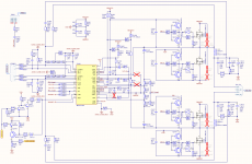
It is based on IRAUDAMP23 (schematics attached). The MOSFETs in schematics have been replaced by IPP530N15N3GXKSA1 which have much lower Gate capacitance.
I have a problem with shoot-through when the high-side MOSFET turns off (and low-side MOSFET turns on).
Although I have gate buffers installed, the driver inside the IRS first seems to slowly discharge to VBoost and then discharges the gate(or the gate buffer transistors) faster. Due to this slow discharge, I get a shoot-through.
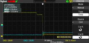
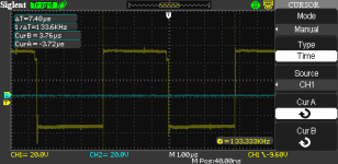
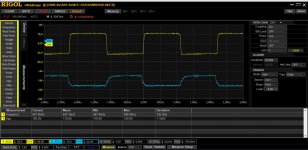
See attached photos taken between R1409 and R1408(yellow) and R1419 and R1424(blue).
Any idea what could be the root cause ?
VBoost is 45V, -VBoost -45V - the other voltages are okay as well (the amp plays well but idle current is too high).
Regards,
Beetlebuster
I have created an amp based on IRS2452 which is design-wise very similar to IRS2092 (has differential inputs).
It is based on IRAUDAMP23 (schematics attached). The MOSFETs in schematics have been replaced by IPP530N15N3GXKSA1 which have much lower Gate capacitance.
I have a problem with shoot-through when the high-side MOSFET turns off (and low-side MOSFET turns on).
Although I have gate buffers installed, the driver inside the IRS first seems to slowly discharge to VBoost and then discharges the gate(or the gate buffer transistors) faster. Due to this slow discharge, I get a shoot-through.
See attached photos taken between R1409 and R1408(yellow) and R1419 and R1424(blue).
Any idea what could be the root cause ?
VBoost is 45V, -VBoost -45V - the other voltages are okay as well (the amp plays well but idle current is too high).
Regards,
Beetlebuster
Attachments
Because it was in the IR2452AM reference design.
I also tested after removing them but it did not improve the results.
I also tested after removing them but it did not improve the results.
Hi,
Did you purchase the Mosfets from Farnell or ebay ?
It is hard to determine from the traces what the time/div is set to.
Is the signal turning on and off the gates timing correct ?
Regards,
Shadders.
Did you purchase the Mosfets from Farnell or ebay ?
It is hard to determine from the traces what the time/div is set to.
Is the signal turning on and off the gates timing correct ?
Regards,
Shadders.
Assuming your plot depicts the hi-side gate. This looks to me like the first falling step indicates full gate turn-off. The following plateau (dead-time) shows output capacitance holding full pos voltage while both hi-side and lo-side MOSFETs are turned off. Followed by hard turn-on of low-side, discharging output capacitance... This is a lossy transition, producing increased power consumption.
Furthermore I assume your output is not connected to an LC-filter, explaining the lack of magnetizing current that would discharge output capacitance during dead-time - and reduce losses significantly.
Just my 2c😉
Furthermore I assume your output is not connected to an LC-filter, explaining the lack of magnetizing current that would discharge output capacitance during dead-time - and reduce losses significantly.
Just my 2c😉
Last edited:
Hi,
I have created an amp based on IRS2452 which is design-wise very similar to IRS2092 (has differential inputs).
It is based on IRAUDAMP23 (schematics attached). The MOSFETs in schematics have been replaced by IPP530N15N3GXKSA1 which have much lower Gate capacitance.
I have a problem with shoot-through when the high-side MOSFET turns off (and low-side MOSFET turns on).
Although I have gate buffers installed, the driver inside the IRS first seems to slowly discharge to VBoost and then discharges the gate(or the gate buffer transistors) faster. Due to this slow discharge, I get a shoot-through.
See attached photos taken between R1409 and R1408(yellow) and R1419 and R1424(blue).
Any idea what could be the root cause ?
VBoost is 45V, -VBoost -45V - the other voltages are okay as well (the amp plays well but idle current is too high).
Regards,
Beetlebuster
The drive circuit seems strange can you bypass it altogether. would recommend next you use DiodesZetex ZXGD3003E6TA. The waveform looks like storage charge coming from the drive circuit.
Hi MOSFETs are from Farnell, timing is set to 100ns/DIV as depicted in the lower area of the screenshots.
Hi,
Did you purchase the Mosfets from Farnell or ebay ?
It is hard to determine from the traces what the time/div is set to.
Is the signal turning on and off the gates timing correct ?
Regards,
Shadders.
Hi Bucks,
yes, the yellow trace is the high side gate, the blue is the low side gate.
Your explanation sounds plausible to me - looks like there is even "too much" deadtime ;-)
There is a output inductor 10uH output inductor but only a 470nF capacitor (and no snubbers) because I did not have larger ones. Should I increase the 10uH to get more magnetizing current ?
Regards,
Beetlebuster
Assuming your plot depicts the hi-side gate. This looks to me like the first falling step indicates full gate turn-off. The following plateau (dead-time) shows output capacitance holding full pos voltage while both hi-side and lo-side MOSFETs are turned off. Followed by hard turn-on of low-side, discharging output capacitance... This is a lossy transition, producing increased power consumption.
Furthermore I assume your output is not connected to an LC-filter, explaining the lack of magnetizing current that would discharge output capacitance during dead-time - and reduce losses significantly.
Just my 2c😉
beetlebuster said:..looks like there is even "too much" deadtime..
I think that applies to after the low-side turn-off transition (but before the high-side turns on), when the commutation current clamps the output node to the +ve rail, due to the "long" dead-time.
However, as per your previous post, the high side (yellow) seems to be turning off instead, in which case the expected dead-time clamping is expected to be towards the negative rail....?
Last edited:
Dear Beetlebuster,
On second thoughts, I think you may be right, as the clamping polarity is also dependent on load current direction.
That is, if your screenshots correspond to negative load current (inward power flow), then the high-side body diode would remain active (clamp the output to positive rail) even after the MOSFET channel has turned off. Once the (long) dead-time has elapsed, the low-side device turns on, pulling the output low, also charging the inductor to repeat the cycle.
So yes, keeping the dead-time small will reduce body-diode clamping activity to give a more "textbook-like" waveform.
No, increasing output inductance will reduce magnetizing current. Do not change your output filter.Should I increase the 10uH to get more magnetizing current ?
Regards,
Beetlebuster
Measuring output current using a magnetic coupler is very enlighting. Poor mans solution is simulating with LTSpice😉
The drive circuit seems strange.
I agree.
Im using a driver circuit like the attached pdf.
I'm using FZT853 and FZT953, the switching frequency is about 550 kHz
I'm not using the chip that the OP is using, but my own discrete design.
The ZXGD3003E6TA seems like a good candidate, nice catch.
I'll have to try it.
BTW as "bucks bunny" says, you should not increase tho output inductor.
Stein
Attachments
I agree.
Im using a driver circuit like the attached pdf.
I'm using FZT853 and FZT953, the switching frequency is about 550 kHz
I'm not using the chip that the OP is using, but my own discrete design.
The ZXGD3003E6TA seems like a good candidate, nice catch.
I'll have to try it.
BTW as "bucks bunny" says, you should not increase tho output inductor.
Stein
I would also recommend a glitch filter to go with it, The aim would be to build a high quality robust driver circuit and have the front end take the hit if destruction occurs and function as a filter against destructive states leaving the chip (the chip does have some of this built in I think)...its possible to create a shoot through condition just by touching the the traces.
US8487647B2 - Circuit and method for deglitching an input signal
- Google Patents
beetlebuster is it the actual ref design board you are using?
Are you sure you actually have shoot through? ... the fets should heat up quite some.
Have you played with the delay time (2 res connected to DT pin)?
IPP530N15N3GXKSA1 is a super easy load with Ciss less than 700 pF. You can easily drive these without the buffers on the IRS2452.
If you really have shoot through you should also be able to measure this using a small series resistor in one of the rails and using 2 probes in diff mode.
The output coil, if it is the same type as used on the ref board, will probably run somewhat hot at +-45V supply. The core is not lowloss and or big enough, but will still work. For anything more than +-35V I would go for a good T106-2 core, but that is a different matter.
What is the actual switching freq? On picture 2 it looks like 133 kHz?
This is way to low, go for ca 350-400 kHz, especially with a filter of only 10uH/470nF.
I'm always using 22 uH / 1uF for my designs.
A higher freq will also have a positive effect on the core/coil losses.
Do you have sound through?
Pictures of board + supply?
Hi Baldin,
actually I do some kind of mix between IRAUDAMP23 and some IR2092-based eval board.
Yes, I played around with the deadtime and lowering it caused the MOSFETs to get hot.
Frequency is set to 300kHz now but for the measurements I reduced it to 130kHz but the issue also happens at 300kHz.
I have sound output.
But the idea with the resistos is a good one - I will try this and also send you photos as soon as I am back in the workshop.
Thanks a lot for your support, everybody.
Regards,
Sebastian
Hi,
Are the gate driving transistors inserted correctly ?
I have made an error with a dual transistor SMT by getting the pins wrong - it was easy to do at the PCB software package stage.
What does seem odd is that the high gate drive has a small 10volt step which i assume is the turn off HO2, then only when the LO2 drive is activated at the end of the dead time, does it look like the upper MOSFET turns off and hence you get shoot through.
Regards,
Shadders.
Last edited:
Beetle,
Is it possible to show the high-side MOSFET's gate voltage with respect to its source (Vout node)? That should clearly tell you what switches when and also whether dead-time is indeed the issue.
Is it possible to show the high-side MOSFET's gate voltage with respect to its source (Vout node)? That should clearly tell you what switches when and also whether dead-time is indeed the issue.
Hi beetlebuster
I still do not entirely understand what the issue you are facing is?
- Do you actually see/meassure a high idle current with large spikes to suggest shoot through?
- Does the fets get hot?
- Does the filter coil get hot?
Start by setting the deadtime high, by connecting DT pin to COM (Negative rail) through a resistor of less than 10k.
I would also think that what you are measuring at the gate is somewhat a function of the Gate input being a rather complex load
I would also still overall recommend a Fs around 400 kHz .... but for now figuring our to get it to actually work ok, 300 will be ok 😉
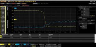
Out of curiosity I just measured on my amp board here on my table.
Running a bit more then 400 kHz
No heat sink at all, all cool and good 😉
But as you can see the gate voltages are maybe not exactly what you would expect. (lower gate a bit noisy but this is just measurement artifacts ... GND coupled to the other probe).
These are IRFB5620 fets.
The fets you are using are the newer Optomos3 types which have quite complex gate capacity. I struggled for a long time making the IPP320N20N3 (also optimos3) fets behave and have now given up. They tend to give a lot of ripple.
How does your output switching look??
Attachments
Dear beetlebuster,
I'm facing the same problem as you. Please let me know if you could find the cause of this problem. I found that the prolonged decline of the upper shoulder does not always manifest itself, a series of prolonged recessions alternates with a series of rapid ones. I have an assumption that transistors in the gate buffer do not always open. But I can't find the reason for this phenomenon.
I'm facing the same problem as you. Please let me know if you could find the cause of this problem. I found that the prolonged decline of the upper shoulder does not always manifest itself, a series of prolonged recessions alternates with a series of rapid ones. I have an assumption that transistors in the gate buffer do not always open. But I can't find the reason for this phenomenon.
- Home
- Amplifiers
- Class D
- Dead-Time issue with IRS2092/2452AM