i have built around 30 sets of these leach superamps since 1984 and i never had any offset voltage greater than +/-100mv in any of them, like mr leach i never matched any components, i believe the input stages must have the correct voltages in the first place to stablish the desired quiscient points as per design....anyway, what i do during testing is to use 10ohm,1W resistors in liue of the fuses, that way i can do idle current setting, voltage offset checking, without fear of losing my output transistors in case of wiring errors..as for errors, common ones i encountered are reversed bias diodes, you will be amazed at how fast you can fry your output transistors this way....so the 10ohm,1W resistor is an important tool for me.....
Alright guys, I guess I'll just fire it up and see what happens. (I hope not literally) It still seems strange to me that there would be such drastic differences between the two boards (which should be identical) but we'll see what happens.
BTW, I do have access to a variac so I hopefully can avoid any major problems. But I will definitely use the resistors instead of fuses. Are there any other suggestions as to what I should look for? (this is my first time doing this) Or just suggestions on this process in general that you guys have gained from experience? Do I just test the DC voltages on the boards themselves, or is there some other point I should look at?
Your suggestions are very welcome and helpful.
Thanks,
Wes
Joan2,
I take it then that you didn't conduct tests on the individual boards before installing them in the chassis and to the output transistors etc?
I take it then that you didn't conduct tests on the individual boards before installing them in the chassis and to the output transistors etc?
no, i did not, i just checked and double checked everything, it would be nice if you can have somebody check your work before you apply power....however those 10ohm resistors saved from a lot of grief!!! i went ahead and mounted the boards after i am confident i did everything right, then i got my 10 ohm resistors, i am using a heatkit sine-square wave generator and dummy loads resistors for checking....you can solder the 10ohm resistors onto a busted fuse, then slap them into the fuse block and off you go...if there were no smoke after powering up, then congratulations, if there was try to find the problem, could be reveresed diodes mostly....good luck!!!
wrl, since the driver seems to consume normal amount of power, apply nominal voltage (or at least minimum voltage), then you can make conclusions.
But first (iyou can), calculate all currents and voltages.
Assume 0.7 V Vbe and Hfe 300 for all small signal transistors and 100 for the driver transistors. With this simplification you can calculate almost everything.
But first (iyou can), calculate all currents and voltages.
Assume 0.7 V Vbe and Hfe 300 for all small signal transistors and 100 for the driver transistors. With this simplification you can calculate almost everything.
What do Vbe and Hfe mean? Is the the voltage and current between the base and emitter? Also when you say all currents and voltages do you mean everywhere on the board or just at every transistor? Finally, just to be sure I am doing things correctly, to measure the dc offset I just connect a multimeter between output and ground. Correct?
Sorry I'm a newbie.
Thanks a lot for your help.
Wes
Sorry I'm a newbie.
Thanks a lot for your help.
Wes
Yes, Vbe is the voltage between base and emitter and this voltage is rather constant. Hfe is the current gain. You can forget that the collector current is not exactly the same as the emitter current.
(collector current = bas+emitter current)
With this you only have to know Ohm's law.
If you have a 10 MOhms (input impedance) multimeter you can measure anywhere.
The output offset voltage is simply the DC voltage you have on the output when you have no input signal.
Don't be sorry for being a newbie. DIY is fun and you must start somewhere. I started when I was 12 and back in those days there was no internet. I had noone to ask.
wrl,
since the offset seems to get higher as you increase the voltages, better check your zeners, one could have been installed backwards....
since the offset seems to get higher as you increase the voltages, better check your zeners, one could have been installed backwards....
wrl, do you have the opportunity to take a picture of the pcb? Lot's can be seen only by looking at a picture.
Pictures:
I do have the ability to take pictures, I'll do it as soon as I get time + post them.
I'm pretty sure my zeners are all oriented correctly as I've checked this many times (although that doesn't mean its for sure 🙂 )
I am now leaning more toward a possible short in the traces (because I made the boards myself and yes, it was my first time) or a malfunctioning part rather than assembly error. Although I have also checked for these many times as well.
I really appreciate all of your help, I don't know how peranders could have done it with out something like this forum.
Thanks
Wes
pretty hard to check for component failures when they are wired in; e.g., a 10k resistor is not necessarily going to measure 10k when it is connected to others. Best you can do is compare measurements to a working board. I wouldn't be too focussed on the offset right away. I WOULD check very thoroughly for solder bridges, though. To test, put in a sine wave and observe the output. The tops of the waves will not be fully rounded until the PS voltage is raised high enough. I thought that Leach specified this procedure. Unless you are getting clean sine waves, don't concern yourself with offset.
I noticed some offst behaviour with my amp that I thought was odd. If I recall, I measured the offset with the inputs shorted, and got around 300mv (which blew me away, because I very carefully matched everything). When I removed the short from the input, the offset went down to 10mv or so. (I hope I remember that story correctly-it's been over 5 years.) Never did figure that out.
I noticed some offst behaviour with my amp that I thought was odd. If I recall, I measured the offset with the inputs shorted, and got around 300mv (which blew me away, because I very carefully matched everything). When I removed the short from the input, the offset went down to 10mv or so. (I hope I remember that story correctly-it's been over 5 years.) Never did figure that out.
Re: Pictures:
I was very thourough back in those days. I did exactly as the schematic and turned every part right. The amp worked at first power on! If anybody want to check, search for a databook from Philips with AD161 and AD162. In this databook from the 70's there was also a amplifier with BC547, AC128/01 (the one with rectangular body), AD161, AD162. 8 watts in mono. My happiness was near nirvana.....
If you suspect some short you simply measure with your DVM (Ohm or Continue check) and if it reads 0.0 ohms or 0.4 (maybe, wires included) then you probably have a short. And of course, you must have switched off the voltage COMPLETELY.wrl said:I really appreciate all of your help, I don't know how peranders could have done it with out something like this forum.
Thanks
Wes
I was very thourough back in those days. I did exactly as the schematic and turned every part right. The amp worked at first power on! If anybody want to check, search for a databook from Philips with AD161 and AD162. In this databook from the 70's there was also a amplifier with BC547, AC128/01 (the one with rectangular body), AD161, AD162. 8 watts in mono. My happiness was near nirvana.....
Pics Pics Pics
Upon further inspection, I found no solder bridges or wrong parts. For all I can observe, the boards are identical.
The output was a clipped sign wave. The only reason I became suspicious was because the output to the other board was a "nonclipped" sign wave at the same voltage. And when I unbalanced the +- voltages, the output became "unclipped".
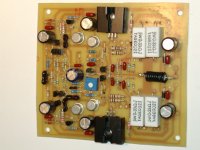
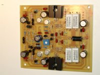
If there are any other pics that would be helpful just let me know. I also have pics of the backside of the boards with the traces.
Thanks,
Wes
Thanks,
Wes
Did you prep the boards like Leach specified in his instructions 1) and 2) at:
http://users.ece.gatech.edu/~mleach/lowtim/part2.html
under "Testing the Circuit Boards"?:
1) Temporarily tack solder two 100 ohm resistors to the back of each circuit board, one from the loudspeaker output to one side of R36 and the other from the loudspeaker output to the other side of R36.
2) Tack solder a short circuit jumper in parallel with C12.
3) Connect the positive, negative, and common outputs from a dual power supply to the board. Note that there are two circuit board grounds to which the power supply common must be connected, one is near the input and the other is near the output. The power supply output voltages should be set to zero and the current limits should be set to about 50 mA. If the power supply does not have a current limit function, connect a 100 ohm 1/4 watt resistor in series with the positive and negative power supply leads.
4) With a signal of about 1 V peak at 1000 Hz connected to the input and a dc coupled oscilloscope connected to the output, slowly turn up the power supply voltages. The circuit should amplify without drawing more current than about 25 mA when the power supply voltages are about 8 V dc or greater, not to exceed 60 V dc. The output signal will initially be a clipped sine wave until the power supply voltages are increased.
If you have more than 25ma, you probably have a building error and need to stop and find it. If the current draw is OK, raise the supply voltage while observing output waveform. As the voltage is raised the sine wave should get better until it pops in. If that doesn't happen, check harder for wiring errors. Check carefully for solder bridges across traces where they shouldn't be. They can be real difficult to detect, because they can look like real traces. Check carefully that you have your transistor leads oriented properly. These are real easy to screw up. I usually put an alligator clip on the transistor lead between the board and the case to draw heat away from the case while soldering the leads, to prevent burning up the transistor.
I think the first step is to raise the voltage and observe the current draw and sine wave. You haven't yet determined for sure whether or not you actually have a problem.
Also, check polarity of caps, and make sure you haven't switched PNPs for NPNs. Obvious, yes, but it happens. Check operating voltages at various points in your circuit, e.g., across zeners, the tail resistors in the input stage, etc., and all power supply traces. If you tacked the resistors in to test, make sure they are tacked properly, and not shorting anything out. If all else fails, try removing some of the protection transistors, to see if they are shorted and limiting.
My power supply doesn't provide more than +-20V, but at this voltage the amp didn't seem to be drawing any observable current. (just to be sure that the current meter on my PS isn't broken, is there a way I can measure this with an multimeter?)
I think that I might possibly have burned out a transistor while soldering them in because I felt them get pretty hot. To check for this I can just measure Vbe and Hfe for the transistors right?
Thanks,
Wes
I think that I might possibly have burned out a transistor while soldering them in because I felt them get pretty hot. To check for this I can just measure Vbe and Hfe for the transistors right?
Thanks,
Wes
- Status
- Not open for further replies.
- Home
- Amplifiers
- Solid State
- DC offset problems with leach amp