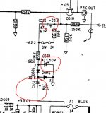
Those readings are odd. How is the gate of the FET at 19.8 volts if point E is only 0.598V? It should only be at 0.5V.
These amps often have earthing problems, usually a buzz on one channel. Measuring a voltage at points A,B,C without the cap and FET suggests there's a weak earth connection. Try moving the -ve meter lead around different earth points in the amp and see if you get different readings; chassis, phono connector earths, different PCB earth planes etc.
I don't like this mute circuit, it uses a switch contact on the mains switch, a bit too close for comfort. The later 3020i had a different arrangement, much safer. The circuit is at hifiengine, 3020i_3225PE.
I wonder......
Check if the minus 62 volts is present here. The two lower caps could be suspects.
I'm wondering if the voltage readings are true or whether there could be an AC component to them that a meter can't show.
A high positive peak voltage (that a meter can't resolve but an oscilloscope would) could conceivably drive enough current through the 10Meg and 100k to create a significant offset.
Attachments
This is getting stranger but very interesting...
We'll pick up from this point:
There are a couple of totally different possibilities for what is happening so lets explore each.
We have to go back to the basic theory of how the FET operates and what it does. The FET turns on when the gate is brought toward zero volts. That allows the FET to conduct and pass the audio. It operates as a simple on/off switch. That is the normal condition when the amp is on.
When the gate is taken negative, the FET turns off and mutes the audio.
So far so good. If the gate is taken to far positive then the gate channel of the FET will conduct and allow gate current to flow (which we don't want). That current allows the offset voltage to appear. So the gate needs to operate within strict limits. No more than around 0.3 volts positive (so the FET doesn't allow DC current to flow and cause an offset).
1/ The 19 volts you measure on the gate of the FET is a problem. So much so that I wonder if you have reversed points D and E in the measurement. If that has occured then we might be some way to explaining the odd results.
19 volts could allow a significant offset to develop as that voltage is high enough to force enough current through the 10 Meg resistor, through the FET and onto the output line.
That theory only holds good if you have points D and E mixed and so we need to prove that.
Leaving the FET's removed can you now remove the diode D507 (just lift one end of it).
Now check the DC voltage on the two 10meg resistors. They should be floating and have no real voltage present apart from stray pickup. Measure on both ends of each and be sure.
Now measure the DC voltage at the point where the diagram shows -20.8 volts which just below Q510 on the diagram.
I'm guessing that point will in fact read plus 19 volts or so. Can you confirm that is so ?
We'll pick up from this point:
Ok great. So cap and FET removed. So yes, indeed there is no voltage at those points. Eagerly awaiting the next step!
There are a couple of totally different possibilities for what is happening so lets explore each.
We have to go back to the basic theory of how the FET operates and what it does. The FET turns on when the gate is brought toward zero volts. That allows the FET to conduct and pass the audio. It operates as a simple on/off switch. That is the normal condition when the amp is on.
When the gate is taken negative, the FET turns off and mutes the audio.
So far so good. If the gate is taken to far positive then the gate channel of the FET will conduct and allow gate current to flow (which we don't want). That current allows the offset voltage to appear. So the gate needs to operate within strict limits. No more than around 0.3 volts positive (so the FET doesn't allow DC current to flow and cause an offset).
1/ The 19 volts you measure on the gate of the FET is a problem. So much so that I wonder if you have reversed points D and E in the measurement. If that has occured then we might be some way to explaining the odd results.
19 volts could allow a significant offset to develop as that voltage is high enough to force enough current through the 10 Meg resistor, through the FET and onto the output line.
That theory only holds good if you have points D and E mixed and so we need to prove that.
Leaving the FET's removed can you now remove the diode D507 (just lift one end of it).
Now check the DC voltage on the two 10meg resistors. They should be floating and have no real voltage present apart from stray pickup. Measure on both ends of each and be sure.
Now measure the DC voltage at the point where the diagram shows -20.8 volts which just below Q510 on the diagram.
I'm guessing that point will in fact read plus 19 volts or so. Can you confirm that is so ?
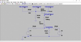
Also... I'm just doing some number crunching on the component values used in the mute circuit and that is leading to the conclusion that what is happening is actually 'normal'. There is no way the gate voltage can be accurately defined, there is no clamp to stop it going positive.
This would (at the time the NAD was current) be considered acceptable and would also assume any partnering equipment was not DC coupled.
I'll explain that in detail later but I think we are chasing a ghost fault here. All is not lost though and there are ways to overcome the issue.
This would (at the time the NAD was current) be considered acceptable and would also assume any partnering equipment was not DC coupled.
I'll explain that in detail later but I think we are chasing a ghost fault here. All is not lost though and there are ways to overcome the issue.
The more I look and the more it seems normal.
Resistive divider R547 and R548 generate a relatively high gate voltage at their junction. In theory that should be one half the applied voltage... maybe your 29 volts is a little high.
So we have around 15 volts generated, and that is applied to the FET's via the 10Meg.
Very approximately... 19 volts across 10 meg generates a current of 0.0000019 Amps. That current flows in the 100k R539 and develops a voltage of 0.0000019 * 100,000 which is 190 mv. You mentioned 200mv in post #1
The numbers are a good fit.
This is going to be normal behaviour I think.
The negative rail (the -62) is applied is applied only at switch on (that auxiliary contact on the switch) and once that opens the negative rail is effectively out of circuit as cap C531 will not affect the DC conditions.
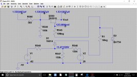
I think this might work as a possible fix.
If you add a high value resistor such as a 1Meg as shown here, and a diode clamp to limit the positive voltage to no more than 0.6 volts then that would limit the gate voltage.
Ideally the diode needs to be a germanium type that has a low forward voltage of around 0.2 volts. If that isn't available then try a small signal silicon, preferably a Shottky type.
The other option is to further AC couple the output with another cap.
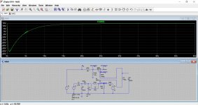
This is a working simulation showing the original and then the modified.
Back later 😉
Resistive divider R547 and R548 generate a relatively high gate voltage at their junction. In theory that should be one half the applied voltage... maybe your 29 volts is a little high.
So we have around 15 volts generated, and that is applied to the FET's via the 10Meg.
Very approximately... 19 volts across 10 meg generates a current of 0.0000019 Amps. That current flows in the 100k R539 and develops a voltage of 0.0000019 * 100,000 which is 190 mv. You mentioned 200mv in post #1
The numbers are a good fit.
This is going to be normal behaviour I think.
The negative rail (the -62) is applied is applied only at switch on (that auxiliary contact on the switch) and once that opens the negative rail is effectively out of circuit as cap C531 will not affect the DC conditions.
I think this might work as a possible fix.
If you add a high value resistor such as a 1Meg as shown here, and a diode clamp to limit the positive voltage to no more than 0.6 volts then that would limit the gate voltage.
Ideally the diode needs to be a germanium type that has a low forward voltage of around 0.2 volts. If that isn't available then try a small signal silicon, preferably a Shottky type.
The other option is to further AC couple the output with another cap.
This is a working simulation showing the original and then the modified.
Back later 😉
Attachments
Ok thanks. I'd like to say that makes sense but that's way beyond what my peanut brain can handle! I'll stop removing bits and look at doing the possible fix. I'll go get the parts and will report back. Thanks so much for all your help so far! Really appreciated.

Only just seen this thread - I think it's 'normal' for ca. 200mV at the pre-amp outputs - I'm actually just measuring a 3120 I'm about to rebuild, and I have +182mV & +198mV at the pre-amp outputs (main amp DC offsets are both <5mV).
If I remember correctly, the schematic also has the switch (SW-1c) drawn in the wrong position on the schematic - it should be open when the amp is ON (not closed as shown). I think the idea is, when the amp's turning off, the sudden high negative voltage drives both JFET's closed, and provides the muting. The caps in the muting circuit are also prone to failure - they are under spec'ed on voltage.
If I remember correctly, the schematic also has the switch (SW-1c) drawn in the wrong position on the schematic - it should be open when the amp is ON (not closed as shown). I think the idea is, when the amp's turning off, the sudden high negative voltage drives both JFET's closed, and provides the muting. The caps in the muting circuit are also prone to failure - they are under spec'ed on voltage.
No problem - I just checked your modification as well, using a 1Meg + 1N4148. The +182mV & +198mV I had last night, are now ca. 1.8 - 2.0mV when they settle down.
The amp needs a full recap, among other things, so I'm loath to comment too much on the 'muting' performance as such, but at the moment both JFETs open together at ca. 4-5" after turn on, and shut off cleanly. There is some transient voltage offset just after the first turn on, that settles after 30" or so, that's not there if it's turned off, and then turned on again, so I suspect it's just cap related (I'll look again after it's rebuilt).
I did also check the SW-1c switch, it's indeed CLOSED when the amp if OFF, and OPEN when it's ON, it's not how it's drawn on the schematic. I'd be interested to see the voltages as it's switched ON, OFF, if you still have the LTSpice model & the time 😉
Looks like it'll be a handy modification.
So...
The switch appears to be used to discharge the cap C531 so that the circuit always functions correctly at power on.
One problem with simulation is that leakage currents in semiconductors aren't always modelled accurately. The original circuit seems to rely on leakage in D507 to 'pass' the negative voltage onto the FET gates. If you look, it is reverse biased and so in theory should not allow the gate to be pulled negative... but it does in both reality and in simulation.
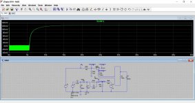
Here is the sim with a real AC voltage source to derive all the voltage. With the circuit in standard form the gate is held negative and then rise positive to unmute.
First image is gate voltage on cathode of D1 in the sim. My mod is out of circuit here. This shows the problem of the unclamped gate voltage that is the cause of the offset.
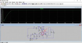
Second image is with the added diode and measuring on the added diode anode. It would seem the gate is not now being pulled negative, presumably due to leakage currents sapping the voltage. The new diode is reverse biased but still pulls the negative voltage down. It does clamp as intended though at around 130mv (shottky diode).
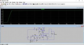
Image 3. Shorting the original D507 out allows the negative voltage to develop. Hmmm ! Should we deliberately make it more leaky with a resistor ?
The switch appears to be used to discharge the cap C531 so that the circuit always functions correctly at power on.
One problem with simulation is that leakage currents in semiconductors aren't always modelled accurately. The original circuit seems to rely on leakage in D507 to 'pass' the negative voltage onto the FET gates. If you look, it is reverse biased and so in theory should not allow the gate to be pulled negative... but it does in both reality and in simulation.
Here is the sim with a real AC voltage source to derive all the voltage. With the circuit in standard form the gate is held negative and then rise positive to unmute.
First image is gate voltage on cathode of D1 in the sim. My mod is out of circuit here. This shows the problem of the unclamped gate voltage that is the cause of the offset.
Second image is with the added diode and measuring on the added diode anode. It would seem the gate is not now being pulled negative, presumably due to leakage currents sapping the voltage. The new diode is reverse biased but still pulls the negative voltage down. It does clamp as intended though at around 130mv (shottky diode).
Image 3. Shorting the original D507 out allows the negative voltage to develop. Hmmm ! Should we deliberately make it more leaky with a resistor ?
Attachments
You're about on my limit now - I'll need to study & digest it a bit.
In the mean time, the 'best' (as far as I can tell !) interpretation of the circuit, that I've seen, is post #53 in the following thread - worth a read I think.
The “VOLKSAMP”
In the mean time, the 'best' (as far as I can tell !) interpretation of the circuit, that I've seen, is post #53 in the following thread - worth a read I think.
The “VOLKSAMP”
Very interesting, thanks 🙂
Its what I would call a bit of 'fringy' design in that it is to reliant on using devices in ways that we wouldn't normally use them.
I had another idea.. and that was to replace my additional diode with a zener instead. That would limit the negative voltage to the zener value.
Its what I would call a bit of 'fringy' design in that it is to reliant on using devices in ways that we wouldn't normally use them.
I had another idea.. and that was to replace my additional diode with a zener instead. That would limit the negative voltage to the zener value.
Attachments
Goldie99, the switch is drawn correctly (SW-1c), all switches are shown in the off position, but not actually off in this case.
I've just checked a 3020A (same circuit) and the pre-amp has an o/p of 6mV, linked or not. A 3020i has 5mV but it's a different circuit.
I've just checked a 3020A (same circuit) and the pre-amp has an o/p of 6mV, linked or not. A 3020i has 5mV but it's a different circuit.
One problem with simulation is that leakage currents in semiconductors aren't always modelled accurately. The original circuit seems to rely on leakage in D507 to 'pass' the negative voltage onto the FET gates. If you look, it is reverse biased and so in theory should not allow the gate to be pulled negative... but it does in both reality and in simulation....
I believe you know this, but....
The reverse leakage of diodes is almost always much larger than the reverse leakage of a JFET Gate.
Diodes are scaled and doped for good forward conduction. The reverse leakage is normally low enough for most diode applications.
The JFET's big feature is HIGH input impedance. And they "never" run the gate forward-biased (much). The gate is scaled and doped, not for forward conduction but for low reverse current. The gate current is specified, and is often a Boast Point on the datasheet.
Millions of audio paths use the '914/'4148 diode in series to a JFET gate and work happy without parts selection.
SPICE will show this, if the models include all the data. Yes, an awful lot of models are approximate in the "normal range" and way-out when you wander to extremes. SPICE needs a good value of IS, but this is not easy to measure and never specified. Model-makers who take defaults for most parameters leave us models that don't cover the extremes.
Thanks PRR. I wasn't sure how accurately LTSpice modelled this although using different diodes seem to give basically similar results.
For this design, the final offset you see at the FET output will depend totally on what is connected to either side of the FET (D and/or S) and this seems to be the function of the 100k on the input side of the FET. The less leakage current that diode has and the lower the offset will be.
I wouldn't class this as good design.
Goldie99, the switch is drawn correctly (SW-1c), all switches are shown in the off position, but not actually off in this case.
I've just checked a 3020A (same circuit) and the pre-amp has an o/p of 6mV, linked or not. A 3020i has 5mV but it's a different circuit.
Spandrel - thanks, you are of course quite correct. I assume I let myself be confused by the switch position shown (closed = power off), but also with all the voltages in that area shown (= power on), that or it's early onset ageing...
I just checked a rebuilt 3020A as well, the pre-out offsets are indeed 6.6 & 6.8mV. From what I've seen trying to find a correct schematic for the 3020A however, there were small differences in the voltage divider values on the anode of D507, for the different 3020 variants (R548 values vary - 68k, 100k, 150k), so the 3020A & 3120 are not completely identical, but how significant that is ? I'm inclined to wonder if NAD were not just tweaking a less than 'optimum' muting circuit. I'll check the 3120 more when I've rebuilt it.
Mooly, Spandrel, PRR - thanks - if nothing else, I at least have a much better understanding of how this circuit works 🙂
🙂 I would definitely call it 'less than optimum' but back in the day it was probably fairly advanced with most amps omitting this kind of feature.
For anyone experiencing highish offest it may well just be worth swapping D507 as a first step and seeing if it improves matters. Everything hinges on the leakage of that device, and that to me makes it a non reproducible design because of the known and fixed loading at the other end of the diode. It is to much of a variable quantity.
For anyone experiencing highish offest it may well just be worth swapping D507 as a first step and seeing if it improves matters. Everything hinges on the leakage of that device, and that to me makes it a non reproducible design because of the known and fixed loading at the other end of the diode. It is to much of a variable quantity.
- Status
- Not open for further replies.
- Home
- Amplifiers
- Solid State
- DC offset on NAD 3120 preamp output