1. Wiring. Find some Teflon insulated 20AWG or 22AWG silver plated copper stranded wire on ebay or locally. With that wire everything, I2S, powerI wish there was something else to improve but I don't have idea🙁
supply and signals. It shouldn't be expensive. These are usually wires for military purposes, they are certainly available locally. With that you can even make 230V 50Hz wiring with additional insulation, say several layers of Teflon tape + PET snake skin for mechanical protection. Avoid heat-shrink insulation, except locally for joints.
2. Opamps. For AD1865 the Burson V5 single OPA performed well, the current model is the Burson V6 Vivid. It is more expensive than this wire. OPA1611 is a cheaper variant, slightly better than OPA604. It has a more open sound, more detail. The OPA1611 requires a SOIC8 to DIP8 adapter. From my experience so far, the AD1865 requires a brighter sounding OPA, the PCM63 vice versa.
3. Passive I/V and tube output. But that's really expensive.
Last edited:

Here, for example, I use this kind of wire for wiring, 20AWG. I just got it locally, much cheaper. This is too expensive, especially the postage is killing.
https://www.ebay.com/itm/1838709598...9111X1517312X237dfcb201beefcbb9ba90627f4e212d
https://www.ebay.com/itm/1838709598...9111X1517312X237dfcb201beefcbb9ba90627f4e212d
Last edited:
Has anyone put capacitors C43 and C44 (18-470pF) on the Iout of the PCM63? What are the sound results, is there any measurement with and without those capacitors?
Well done Ra7!!
Now you’ve been bitten by the DAC bug, very hard not to itch… I mean tweak now.

Now you’ve been bitten by the DAC bug, very hard not to itch… I mean tweak now.
Absolutely! I built it stock but have the D1 I/V ready to go 🙂… itch is strong
Didn’t get to listen long last night but first impression was that I felt relaxed
Didn’t get to listen long last night but first impression was that I felt relaxed
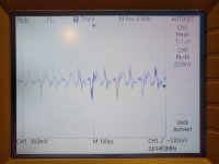
156MHz is a lot for a DAC, it is certainly not the noise of the PCM63 itself, but enters somewhere from the side and spreads through the DAC itself(digital input, power supply, sound source).Here are two pictures of PCM63 DAC measurements. The first is noise at the DAC output and the second is noise at the power supplies. Power supply noise exists on all lines, the same everywhere, on all power lines. The same noise is present on RAW DC as after the regulator. I think it's interference from the environment or from the laptop's power supply, and the box is plastic, so I don't have any protection. I didn't notice the oscillations of the regulator or I can't notice them. 🙄
It is too high a frequency to come from a socket in the wall or the radiation of some device. For comparison, this is noise on the PCM1702, and the culprit for this 3.615MHz is the PMD100 itself. I measured this a long time ago, now with improved regulators the situation is certainly better.
Attachments
3. Passive I/V and tube output. But that's really expensive.
It does not have to be, if you would use JFET instead (active ones, not unobtaniums).
Ask Fran. He might evenhave boards to give away.
🤓
https://www.diyaudio.com/community/...st-tht-i2s-input-nos-r-2r.354078/post-7264114
https://www.diyaudio.com/community/...st-tht-i2s-input-nos-r-2r.354078/post-7264825
https://www.diyaudio.com/community/...st-tht-i2s-input-nos-r-2r.354078/post-7265124
Patrick
Last edited:
I was expecting this answer.
But the post was for the others.
Just worth noting that Fran is happy to put his tube IV aside and use JFETs as his new reference instead.
🤓
Cheers,
Patrick
But the post was for the others.
Just worth noting that Fran is happy to put his tube IV aside and use JFETs as his new reference instead.
🤓
Cheers,
Patrick
I have been attached to tubes since my early youth. 😎
Tubes add a touch of exotics to this DAC. Thinking for now goes in the direction of USB only DAC with JLS, Data L+R directly to PCM63 (skipping the shift registers), then passive I/V with 50ohms, then Mu follower with sufficient voltage gain. I don't know when it will be realized, I'm still studying it.
I'm also planning an Arduino and display with NIXIE tubes which I have plenty of. It will probably take me a year to do it all. 🙄
Lets be fair, tubes, jfets, they are there head to head, it's down to preferences and how well it is made 🙂
Anywho, due to pressure from mikorist and nixie, i made this little bugger especially tailored for @miro1360 dacs and his signature missaligned opamp sockets 😅

Jumpers are there because nixie wants to use both power lanes from both sockets, traces are wider either way, so one can pick their poison. After testing, i'll post gerbers.
Anywho, due to pressure from mikorist and nixie, i made this little bugger especially tailored for @miro1360 dacs and his signature missaligned opamp sockets 😅
Jumpers are there because nixie wants to use both power lanes from both sockets, traces are wider either way, so one can pick their poison. After testing, i'll post gerbers.

Here's the gerber for dual opamp to 2 x mono, i checked the dimensions twice, connections twice, it should work as intended.
Adapter takes both dip8 and soic8 chips.
J1, J2 are jumpers for using both left and right power supply dual lanes. If you need that much copper by nixie request.
SMD pads are for ceramic 1206 capacitors (value that you feel like (0.1uf and up)), for opamp decouple in case it gets unstable due to nature of the adapter and longer lanes. The size was chosen due to ease of hand soldering, so it wont be a problem for anyone.
G is for using ground link to it via cable, in case you use capacitors on adapter. It is above gnd pad on the dac, so it is convenient.
Enjoy.
Attachments
What does better really means for you , and why the TDA 1541 A is overrated , musically speaking 🤔@grunf I can confirm that the PCM1704 NOS (and 1702) is better than TDA1541A, and also AD1862 is better than TDA1541A ... and TDA1540 is also better... In my opinion the TDA1541A is overrated and overpriced
Anyway it is nice to have it in the vintage collection, it is like an old veteran - you won't race it, but you have it in the garage and sometimes you try its seats

.
Hi. I'm building USB DAC using your USB to I2S and AD1862 NOS I2S, but I can't hear anything from the output. My system is Raspberry Pi4(Volumio) USB output > USB to I2s > AD1862 NOS I2S . I changed JP1 & JP2 jumper setting, but there was no luck. In this case, is there any specific jumper settings needed?
Attachments
- Home
- Source & Line
- Digital Line Level
- DAC AD1862: Almost THT, I2S input, NOS, R-2R