AD1860 is something in between and it is 18bit DAC.
But in reality it is 15 bit...
(ENOB=15.3, to be accurate)
1656 (55) - is one of the best.So the opa1655 (and dual 1656) for what DACs were good?
Alex.
It is fast, but not "very fast" - just 3.8MHz Full Power BW, 54MHz GBW, 20MGz Unity Gain and 24v/us slew rate.However, it is a very fast opamp,
Very popular in I/V AD811 - 40MHz Full Power BW, >100MHz GBW and 2500v/uS slew rate.
But you are right - good layout and power bypass required.
However, I have not observed any oscillations with 1656 (with 811 - yes).
Alex.
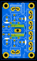
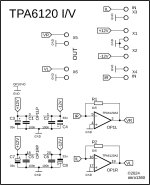
I thought about sharing the I/V based on TPA6120 for a longer time and today I decided to do it 😎
TPA6120 internal structure is pure CFA, it provides an ultra low impedance load for the DAC.
The internal concept is similar to the AD844, but not the same and TPA6120 is 20x cheaper
Is it good I/V? Well, TPA6120 is very fast CFA, sound is super natural and it has a lot of power to drive things
Power supply range is from +-5V up to +-15V. It can be powered directly from DAC PSU.
R1 and R2 value determines the output voltage. For a higher output voltage use higher value of this resistor (1k5 == 1.5Vp, 2k7 == 2.7Vp, ...).
Capacitors are polypropylene and a high quality electrolytics (UKW from Nichicon is still available).
There is hole in thermal pad under the IC, where you solder the IC with PCB from the bottom.
IL, IR is current input from DAC.
VL, VR is voltage output.
If you are worried about damage to the chip due to a short circuit of the outputs, or signal reflection, you can mount 22R series resistors directly on the signal cable.
Note, that a small (not harmful) DC offset may be present in the voltage output.
This is redesigned PCB and so far not tested, I hope it does work.
BOM example: https://mouser.com/ProjectManager/ProjectDetail.aspx?AccessID=5ca5f6fb0b
TPA6120 internal structure is pure CFA, it provides an ultra low impedance load for the DAC.
The internal concept is similar to the AD844, but not the same and TPA6120 is 20x cheaper

Is it good I/V? Well, TPA6120 is very fast CFA, sound is super natural and it has a lot of power to drive things

Power supply range is from +-5V up to +-15V. It can be powered directly from DAC PSU.
R1 and R2 value determines the output voltage. For a higher output voltage use higher value of this resistor (1k5 == 1.5Vp, 2k7 == 2.7Vp, ...).
Capacitors are polypropylene and a high quality electrolytics (UKW from Nichicon is still available).
There is hole in thermal pad under the IC, where you solder the IC with PCB from the bottom.
IL, IR is current input from DAC.
VL, VR is voltage output.
If you are worried about damage to the chip due to a short circuit of the outputs, or signal reflection, you can mount 22R series resistors directly on the signal cable.
Note, that a small (not harmful) DC offset may be present in the voltage output.
This is redesigned PCB and so far not tested, I hope it does work.
BOM example: https://mouser.com/ProjectManager/ProjectDetail.aspx?AccessID=5ca5f6fb0b
Attachments
This is redesigned PCB and so far not tested, I hope it does work.
I see some violations of the "CFA OP usage" rules.
Everything connected to 5 and 16 legs should have a minimum capacity to the ground. Otherwise, there is a high chance to get oscillation - this is CFA..
It is better to make these lines not so thick, shorter and with a higher gap between them and the ground polygons. Usually such lines are on the top, and ground polygon at the bottom have cuts under these legs and connected lines.
Alex.
Thanks @altor for your input 🙂
I know about this capacitance and have done more devices in the past with the TPA6120 where I omitted the GND under the entire feedback path, another device where it was omitted only under the feedback leg, and devices where the GND plane is present .... but I didn't observe any oscillations and TPA seems to be stable ... the parasitic capacitance is around 25 femto in this case. This is more valid to GHz devices. I gradually dropped from that seriousness in audio devices as there are working amplifiers completely without GND plane 🤣
I know about this capacitance and have done more devices in the past with the TPA6120 where I omitted the GND under the entire feedback path, another device where it was omitted only under the feedback leg, and devices where the GND plane is present .... but I didn't observe any oscillations and TPA seems to be stable ... the parasitic capacitance is around 25 femto in this case. This is more valid to GHz devices. I gradually dropped from that seriousness in audio devices as there are working amplifiers completely without GND plane 🤣
Ahhh, this looks familiar Miro 😉.
Another good sounding I/V option. Maybe release the all smd version, much smaller pcb to fit just about anywhere.

Vunce I still haven't overcome the phobia of the MLCC decoupling capacitors for the I/V and opamps 🆘

Hahaha!! 
But, there are nice smt film caps from CDE, Rubycon and Panasonic to help with your phobia.🙂

But, there are nice smt film caps from CDE, Rubycon and Panasonic to help with your phobia.🙂
As this mostly the inductance that matters, I repeat what I already inputed for miro's phobia : There are excellent MKT from Wima with 2.5 m pitch leg, this is what I'd choose in my shoes if I'd stay with tht 0.1 uF decoupling and THT. It doest need to be mkp and at weigthing the poor and con : inductance is more important here than the dielectric ! MKT suffices... imho half illiterate humble opinion and of course YMMV , blah ! 😉
For the people, what are talking V. is talking about is their acrylic line. For the ones wanting an headphone dac that needs a powerfull current buffer for difficult cans : I droped a pcb here with standalone I/V then buffer but with more smd for the decoupling. this is the last folder of this post. All the front end and dac ic layout is from the previous miro1360's JLSOUNDS usb to pcm stacking board. (VFA scheme) : https://www.diyaudio.com/community/...st-tht-i2s-input-nos-r-2r.354078/post-7713233 (seems it had been downloaded 58 times at this day). This is still a two layers optimised. The blue 4 layers is not avaliable and is totally remade about the layout with 4 layers.
Of course as stated, CFA for I/V here will sound different. I input here as this TPA6120 is sometimes chosen for headphones driving as a buffer. Some I/V op amps works better with a dedicated buffer. But the standalone smd version from miro1360 board can works fine also with many cans with an opa1655 as standalone I/V + buffer because its good mA output.
Last edited:
I see that I woke up the ghosts with the AD811, I'm glad about that 🙂.I thought about sharing the I/V based on TPA6120 for a longer time and today I decided to do it 😎
TPA6120 internal structure is pure CFA, it provides an ultra low impedance load for the DAC.
The internal concept is similar to the AD844, but not the same and TPA6120 is 20x cheaper
Is it good I/V? Well, TPA6120 is very fast CFA, sound is super natural and it has a lot of power to drive things
Power supply range is from +-5V up to +-15V. It can be powered directly from DAC PSU.
R1 and R2 value determines the output voltage. For a higher output voltage use higher value of this resistor (1k5 == 1.5Vp, 2k7 == 2.7Vp, ...).
Capacitors are polypropylene and a high quality electrolytics (UKW from Nichicon is still available).
There is hole in thermal pad under the IC, where you solder the IC with PCB from the bottom.
IL, IR is current input from DAC.
VL, VR is voltage output.
If you are worried about damage to the chip due to a short circuit of the outputs, or signal reflection, you can mount 22R series resistors directly on the signal cable.
Note, that a small (not harmful) DC offset may be present in the voltage output.
This is redesigned PCB and so far not tested, I hope it does work.
BOM example: https://mouser.com/ProjectManager/ProjectDetail.aspx?AccessID=5ca5f6fb0b
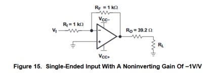
But this scheme lacks two important things, Ri and Ro, which are necessarily recommended by DS. Those two resistors are mandatory with the CFA op amp and you can't get away from them. It would also be good to avoid TH components, except perhaps for large electrolytes, while everything else should be SMD. I agree with Vunce about that.
Attachments
Youu eventually can swap the 1k Ri by a ferrite bead of a near value if you know at what frequency the resistance is needed as @abraxalito inputed.
Added serie resistance is not nice for I/V, but most of VFA op amps have more Zi (but the good ones as opa861 for illustration which is near 17R circa at input... which is one of the first thing of the item list if a good I/V, but you do know choose the good caps to makesit sing and a good enough PS but not sota as the AD811, relative to the dac chip PSRR and noise floor). In fact VFB op amp for that task have their own drawbacks as already talked elswhere.
Of course here it is needed to avoid osci ! Notice the more complex scheme from Walter Young where Ri is inside the feedbackloop iirc (which seemed to me odd before re reading the paper)...
Edit for some reasons here, this input schematic before the CFA whatever the AD811 or this TPA6120 must be smd very close layout for best results. I let the genius of electronic to explain why.
Last edited:
@miro1360 , in the TDA1541A thread, Thorsten Loesch and Zoran have proposed very nice discrete I/V with BJT... and THT 😍 . IIRC @Zoran has proposed already something here btw, do not remember where btw !
The migthy Brijac said he would do separate pcbs with that, btw if not interresting you here for your thread. I haven't planned it myself. Maybe V. at the winter does have the patience, who knows... (support is a b..ch though for most because time consuming)
The migthy Brijac said he would do separate pcbs with that, btw if not interresting you here for your thread. I haven't planned it myself. Maybe V. at the winter does have the patience, who knows... (support is a b..ch though for most because time consuming)
Last edited:
Hope you are talking about their smd acrylic capacitors.But, there are nice smt film caps from CDE, Rubycon and Panasonic
I also used them many times in audio with good results, but not in DACs (were not required, NPO ceramic usually was enough).
Alex.
Last edited:
@grunf I am testing this TPA I/V for 8 years, from 2016, in different configurations 😊
@Vunce The foil SMD capacitors are very fragile during soldering, you can easily damage it with high temperature 🙂 ... The DAC where I would use it is probably only a portable device ... perhaps my easyDAC can have it
@Vunce The foil SMD capacitors are very fragile during soldering, you can easily damage it with high temperature 🙂 ... The DAC where I would use it is probably only a portable device ... perhaps my easyDAC can have it

Altor, Yes we talked about them long time ago in that thread. I disagree though about what you say about them and DAC. Give me wonderfull result with TDA1541A at some areas VS NPO....
Yup 👍🏻Hope you are talking about their smd acrylic capacitors.
I disagree though about what you say about them and DAC.
Of course they can be used in DACs.
I just want to say that I have used these smd film capacitors where I need a few uF of capacitance.
This has never happened in my DACs where I need hundreds of pF or a few nF at most, in the signal pass.
Alex.
😎 @miro1362 ... I have a Proac D15 to sell, I have too much loudspeakers to test all my DACS ! 😁
@altor But the 1 uF CDE, the only acrylic iirc that have more capacitance are the expensive Rubycons...
I use CDE at 0.1 , 0.22 and 1 uF ... I see they are soo NLA (and the ones made by Pany if my memory serves me well which is not often) . I used them with sucess in masterclock with the CDD957, a tweak/tip MarkIV liked and use in his last reclocker board with the Crysteks. And yes it can be heard whatever there are NPO and MLCC in the Crystek metal can. 1UF CDE acrylic at the feet of the Crystek on the power line is working very good. IanCanada used it too after I inputed that on the RPi clock boards with even more uF (22 uF Rubycon iirc, but non only for the Crysteks).
I also use them in my ad1862 4 layers (the blue board of the link above) on the 12V of the AD1862 and on the buffer op amp. I use NPO on the digital side.
@altor But the 1 uF CDE, the only acrylic iirc that have more capacitance are the expensive Rubycons...
I use CDE at 0.1 , 0.22 and 1 uF ... I see they are soo NLA
 (and the ones made by Pany if my memory serves me well which is not often) . I used them with sucess in masterclock with the CDD957, a tweak/tip MarkIV liked and use in his last reclocker board with the Crysteks. And yes it can be heard whatever there are NPO and MLCC in the Crystek metal can. 1UF CDE acrylic at the feet of the Crystek on the power line is working very good. IanCanada used it too after I inputed that on the RPi clock boards with even more uF (22 uF Rubycon iirc, but non only for the Crysteks).
I also use them in my ad1862 4 layers (the blue board of the link above) on the 12V of the AD1862 and on the buffer op amp. I use NPO on the digital side.
Last edited:
- Home
- Source & Line
- Digital Line Level
- DAC AD1862: Almost THT, I2S input, NOS, R-2R


