I have written many times.
When you're using the passive IV with AD797 gain stage,
You MUST remove Riv and Civ from the Miro PCB.
Patrick
When you're using the passive IV with AD797 gain stage,
You MUST remove Riv and Civ from the Miro PCB.
Patrick
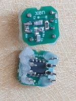
What is the reason for the glue/silicone substance?I soldered the AD797 I/V PCBs....

@EUVLI have written many times.
When you're using the passive IV with AD797 gain stage,
You MUST remove Riv and Civ from the Miro PCB.
Patrick
Thank you!
Now I see.
Just removing Riv Civ and keeping the state opened.
Hi Miro,AD1862, I2SoverUSB v.III - not flipped, 20-Bit uf.l connectors
I2SoverUSB not flipped (pin-headers installed on the bottom side on I2SoverUSB) ... the heatsink and USB connector are on the TOP 🙂
Using "the not flipped PCB version" and the I2SoverUSB v.III powered-up itself. If only H3-9 to H3-16 connected btw both boards, no-touch on SJ1, SJ2 and SJ3, is it correct?
Thanks
@happylistening "I2SoverUSB v.III powered-up itself" -- I assume you mean powered by a USB cable:
SJ1 - close
SJ2 - close
SJ3 - open
Jumper J4 on I2SoverUSB board - close
If you mean powering by itself as powering from an external power supply (not with USB cable from intergrated regulator on I2SoverUSB board), than as you typed: SJ1, SJ2 and SJ3 is open (no-touch), just the jumper on J4 and the respective power supply for I2SoverUSB board.
😉
Last edited:

Quick question before starting on the shunts. What current draw do you see from the AD1862 and the shift registers? I found one post mentioning the 5v shift registers draw ~25ma and each ad1862 seems to consume ~15ma judging from the spec sheet.
Cheers -
Cheers -
I found these numbers in post #234. The seem a bit high but maybe a good start.required current as a rough estimate with a fine reserve, in the reality it is less:
+-200mA for analog (+12V/200mA, -12V/200mA)
+-100mA for digital (+5V/100mA, -5V/100mA)
The current draw is much higher in the +5V supply for an active signal and in the -5V supply it remains unchanged, any ideas why this happens? 🤔5v supply @idle/active signal:
+5V = 5mA/22mA
-5V = 3.3mA/3.3mA
They draw all that current, WOW, from the datasheet it seems much less.
At which frequency were the tests performed?
At which frequency were the tests performed?
I got PCBs in hand and am looking to order parts. Has anyone identified upgrades for the caps on the DAC side of the board (ad1862)? I saw one person substituted the ceramic and polypropylene caps with SMDs.
Cheers, Soren
Cheers, Soren
Particularly curious about the C1-C6 0.1uf ceramic caps and the C9/10/13/14/19/20/23/24 0.1uf PP caps.
If you substitute, go for c0g (np0) ceramic, or go for rubycon MU capacitors. But as zoom said, make it first, then mod 🙂I got PCBs in hand and am looking to order parts. Has anyone identified upgrades for the caps on the DAC side of the board (ad1862)? I saw one person substituted the ceramic and polypropylene caps with SMDs.
Cheers, Soren
- Home
- Source & Line
- Digital Line Level
- DAC AD1862: Almost THT, I2S input, NOS, R-2R