MiroDac boards are useful in more ways than just converting zeros and ones!
Finish sanding with 2000grit and dacblock😂
You are 100% right, I was just trying to figure it out, I will run some simulations on TINA.
BTW your board looks awesome 😎

Sorry, but I really want to do 2 more silly (noob) questions.
When the AD1862 is connected only to the I/V stage, the signal is inverted (180° phase shift)?
Why a reconstruction (anti-imaging) filter is not required?
When the AD1862 is connected only to the I/V stage, the signal is inverted (180° phase shift)?
Why a reconstruction (anti-imaging) filter is not required?
1. Signal voltage is not inverted after this I/V stage because the output from DAC is current (not voltage). But there exists a 180° phase difference between the input current (current from DAC) and output voltage from opamp. How important is that to the system setup when the opamp is the first device which produces the voltage? 🤔
2. There is not one good filter, many variants exists and many can be created and each move the original sound somewhere (some soften the sound, others emphasize the bass, others emphasize the treble, some move the stage forward, others backward) 😁 Which one is the best?
The sound from AD1862 is very good without this filter, actually the sound is perfect and maybe that can be the best reply for the question 😁
Last edited:
Did I share the PCB? If not, here it is 😁Yes they are BRN 😉
Attachments
-
diyAudio_PCM63P_DAC_v1.4_uf.l_jlsounds-notFlipped_align_2022-12-22.zip771 KB · Views: 117
-
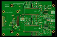 diyAudio_PCM63P_DAC_v1.4_uf.l_jlsounds-notFlipped_align_PCB.jpg511.6 KB · Views: 264
 -
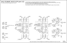 diyAudio_PCM63P_DAC_v1.4_uf.l_jlsounds-notFlipped_align_Schematic1.jpg297.5 KB · Views: 269
 -
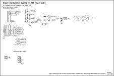 diyAudio_PCM63P_DAC_v1.4_uf.l_jlsounds-notFlipped_align_Schematic2.jpg167.8 KB · Views: 263
Thank you very much, Miro.1. Signal voltage is not inverted after this I/V stage because the output from DAC is current (not voltage). But there exists a 180° phase difference between the input current (current from DAC) and output voltage from opamp. How important is that to the system setup when the opamp is the first device which produces the voltage? 🤔
2. There is not one good filter, many variants exists and many can be created and each move the original sound somewhere (some soften the sound, others emphasize the bass, others emphasize the treble, some move the stage forward, others backward) 😁 Which one is the best?
The sound from AD1862 is very good without this filter, actually the sound is perfect and maybe that can be the best reply for the question 😁
Yes, you're right, since the current phase diference occurs on both channels there is no problem at all.
If the filter affects SQ it's in fact better to skip this stage.
You are 100% right, I was just trying to figure it out, I will run some simulations on TINA.
BTW your board looks awesome 😎
I've run the simulations, everything is working perfectly, I was assuming that the input of the 3rd shift register chip was taken from the 2nd's final output, instead of the 3rd.
Anyway is it possible to use only one data signal and acquire both DL and DR from the 2nd 74HCT164's 3rd output? In this case an inverter (e. g. 74HC04) would be needed for the left latch signal. The advantage, less digital components, the drawback is the added inter-channel delay.
Would this have a significant impact on sound, what do you think?
Can I use the HC version instead of the HCT for the 74x164?
For me, PCM56K is just as good as the AD1862.
And there is hardly any difference in noise level.
DS specs for noise typically are 110dB vs 117dB. Did your measurements reflect that?
@danny92 It is inaudible shift, you can do that. Since you add one inverter, you already have 3 ICs. In that case, it might be better to do my stop-clock solution ... #3969 #4862
Or you can use the CPLD and omit the digital chips altogether: https://electrodac.blogspot.com/p/i2s-to-pcm-dac-converter-tutorial-cpld.html
... my CPLD does stop-clock, does not use MCLK, is probably the easiest way to do it so that it does not process a lot of calculations == even less digital distortion for DACs 😁
... It all depends on your preferences, but the original solution from post #1 is still great and well tested 😊
You need the HCT (it is TTL) ... HC has different input levels (it would have to be converted or dealing with power supplies).
NIXIE tubes is the right way for you. 🤣
This is going into my next DAC. 🤣

Hello @miro1360 these are the instructions for the JLsounds I2SoverUSB on the dac board.
View attachment 1191328
So if i am using two external PS ie. one for USB and one for the clock for the I2SoverUSB , SJ1~SJ3 should be left open?
Yes, SJ1-SJ3 is left open for two external PS. Next you must cut external power supply jumper on the I2SoverUSB board located on the bottom side of the board.
First external power supply for USB side goes on H1.1 and H1.2. Second external power supply to H3.17 (+5VD2 pin) and H3.19 (GND pin) 😉 ... Note that in this option the USB side is not powered from PC, but externally.
Alternatively you can power the USB side from PC (not cutting external power supply jumper on the I2SoverUSB board). Just provide one external power supply for crystals on the +5VD2 pin and GND.

You need the HCT (it is TTL) ... HC has different input levels (it would have to be converted or dealing with power supplies).
Just a curiosity, is the AD1862 compatible with CMOS levels? I think the I2S interface signals, SDATA, BCLK and LRCLK are in fact CMOS level (3.3 V high level). Do you need a level shifter after the USB -> I2S or SPDIF -> I2S converter?
The HC version can also be supplied from a +5V supply, I guess. Regarding the input thresholds they are a bit different (for the HC and HCT versions), so I think I have to use the 74HCT164 or the 74LS164, for interfacing directly with I2S.
Last edited:
- Home
- Source & Line
- Digital Line Level
- DAC AD1862: Almost THT, I2S input, NOS, R-2R