Look what the cat dragged in... everyone owes @diyiggy a round of applause (or drinks) for suggesting an alternate ordering path.
Attachments
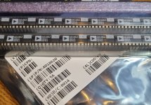

Fantastic Paddy! Great news genuine AD1862 chips are once again available.
Cheers Iggy!!

Cheers Iggy!!
If possible I would gladly take a pair of 1862Look what the cat dragged in... everyone owes @diyiggy a round of applause (or drinks) for suggesting an alternate ordering path.
Those in the EU can GB yourselves :
https://www.digikey.nl/en/products/...1862N/12107023?s=N4IgTCBcDaIIYBMCMAOAbBAugXyA
No need to pay expensive US Post.
Patrick
https://www.digikey.nl/en/products/...1862N/12107023?s=N4IgTCBcDaIIYBMCMAOAbBAugXyA
No need to pay expensive US Post.
Patrick
Someone really should, the postage is 34% of the cost of a pair of chips. I can also work with someone who wants to aggregate - again, PM.
Good news Paddy, a friend still wanting a Miro Dac.
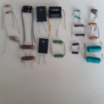
Btw, I am still working on the I/V resistors test. Results quite promising. The ranking starts from not too good that not thanks excellent Miro pcb and AD1862 dac chip to good but non optimal... towards taste of high-end I totally can live with. Hifi brands rarely optimise their work and differences stands also there. So here people share more or less to try to make grow this well born project and good spirit from Miro1360.
It is for simple oaps so still on the cheap... One will be surprise on how big enough is the difference if your hifi is transparent sounding...I am not an easy guy with hifi expectations... It will be a modest yet subjective contribution in the spirit of the thread. Oaps for this test are jfet and bipolar, yet the ranking works for both Oa1656 on @Vunce adaptator pcb dual soic to single DIP8 and the single channel OAP 1611 from TI, cheap cheap...good good sounding.
Attachments
Last edited:
IN EU we now do not Great Britain ourselves ! (I joke they are welcome 🙂 )Those in the EU can GB yourselves :
https://www.digikey.nl/en/products/...1862N/12107023?s=N4IgTCBcDaIIYBMCMAOAbBAugXyA
No need to pay expensive US Post.
Patrick
And for spidf and toslink
https://www.soundimports.eu/en/sure...MabmfG3fk_Z9jeJbqIcKFL1dvZRJxt6oaAk75EALw_wcB
https://www.soundimports.eu/en/sure...MabmfG3fk_Z9jeJbqIcKFL1dvZRJxt6oaAk75EALw_wcB
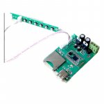
"There is interesting cheap input device on ali: USB/SD/Bluetooth to I2S with control buttons."
A single CSR8675 does everything.
You think it is a good solution ?
😉
Patrick
A single CSR8675 does everything.
You think it is a good solution ?
😉
Patrick
"for spidf"
The simpler the better :
https://www.diyaudio.com/community/...e-new-ess-vout-dac-es9022.151846/post-2861671
"and toslink"
Adds more jitter.
Patrick
The simpler the better :
https://www.diyaudio.com/community/...e-new-ess-vout-dac-es9022.151846/post-2861671
"and toslink"
Adds more jitter.
Patrick
Attachments
That is for thosr with small budget and compact disc still. For sure it is not at the level of a Wave i/o or JLsounds front end. But not the same price either. Yup never liked Toslink either...
Now if one uses it NOS...these chips are less sensitive to jitter than sigma delta chips.
And those I2S plug that add heigth so biggest ground loop, more inductance are not wanted...or at least bad EMC practices.
I am amazed with oap virtual ground the I/V resistor choice can make such dac chips sound natural or totally artificial like first cd players...
In my last AD1865 dac I use TR161 resistors for the I/V.Good news Paddy, a friend still wanting a Miro Dac.
Btw, I am still working on the I/V resistors test. Results quite promising. The ranking starts from not too good that not thanks excellent Miro pcb and AD1862 dac chip to good but non optimal... towards taste of high-end I totally can live with. cheap...good good sounding.
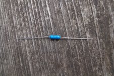
The blue resistors.
Give them a week under stress to settle down.
In the beginning they sound harsh on the high, which later disappears.
I've also tried many different resistors for I/V in the past, nice to see you doing the same.
Attachments
Hi democles,
Thanks, good tip.
The dark blue on my picture is Vishay Dale PTF56 serie 5 or 10 ppm. So I think not the same as yours.
This verry precise Vishay is one of the bad result category in my setup...though only sung 2 hours. In fact none of the little metal films were good... even those with were already broken in. More to come this week as I am double checking the test. But I will come back after with more breakin in in the 100 hours in the year...
The description I found on the net.
TR 161 are resistors of the now defunct TESLA branch in Jablonné. These are quality resistors with a NiChrom layer, non-magnetic, capless, manufactured in a similar way as DALE resistors. They were produced in the E192 series with a tolerance of up to + -0.25% and TK up to + - 15ppm. They come in green and blue - there is probably no difference between the two variants. In my opinion, this is a suitable Czech alternative to foreign production - but their stocks are also limited.
TR 161 are resistors of the now defunct TESLA branch in Jablonné. These are quality resistors with a NiChrom layer, non-magnetic, capless, manufactured in a similar way as DALE resistors. They were produced in the E192 series with a tolerance of up to + -0.25% and TK up to + - 15ppm. They come in green and blue - there is probably no difference between the two variants. In my opinion, this is a suitable Czech alternative to foreign production - but their stocks are also limited.
Attachments
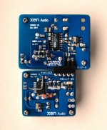
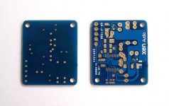
AD1862 Stop-Clock
I did this PCB half year ago and somehow forget to post it here and today found it 🤣
It incorporates the Stop-Clock system. What does that mean? Simply: The BCK (clock) is off while no data are present for DAC chip.
I don't know if it has any positive impact on the AD1862 chip, but only 4 digital chips are on the PCB instead of 6 👍
Another "major" change is in the ground plane on the PCB. I divided the GND plane for digital and analog with thick cut lines. This helps eliminate potential digital interference and can have another positive impact on the sound 🤩
BOM example: https://www.mouser.com/ProjectManager/ProjectDetail.aspx?AccessID=c547c05bf3
note: I/V OpAmp in BOM is LM7171, you can buy another one
The PCB is not tested ...
Attachments
-
diyAudio_AD1862_DAC_v2.0_Stop-Clock_2021-11-25.zip651.7 KB · Views: 133
-
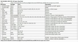 diyAudio_AD1862_DAC_v2.0_Stop-Clock_BOM.jpg206.1 KB · Views: 226
 -
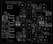 diyAudio_AD1862_DAC_v2.0_Stop-Clock_parts.jpg219.2 KB · Views: 228
 -
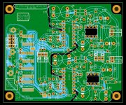 diyAudio_AD1862_DAC_v2.0_Stop-Clock_pcb.jpg406.7 KB · Views: 235
 -
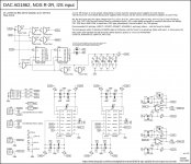 diyAudio_AD1862_DAC_v2.0_Stop-Clock_Schematic.jpg463.3 KB · Views: 261
Thanks Miro.
For learning purpose, what are the order of layer from top to bottom of the board please ?
Top is signal and power traces, gnd islands tied either to signal gnd plane or power gnd plane ?
Second plane is agnd and dgnd (chip ground)
Third plane power gnd ? Tied here and there to chip ground ?
Forth plane is power ground ?
Micro strips tied the local islands on either on the power or chip ground ?
Or power ground and chip ground on the same layer ?
I use the former ufl board that works fine 🙂.
@diyiggy
The PCB stack up ... for this DAC only 2 layer PCB is used. Top layer are signals, power lines and GND filling, Bottom is solid GND. Vias are used for connecting TOP ground fills with solid GND, almost everywhere. This is simple PCB, no science 🤓
You can find more complicated PCBs witch many layers, where some of layers are used as power planes. Google images "PCB stack up".
Good example for 6 layer PCB stack up is like this:
Signal - (prepreg) - GND - (core) - Signal - (prepreg) - Power - (core) - GND - (prepreg) - Signal
or Signal - (prepreg) - Power1 - (core) - Signal - (prepreg) - GND - (core) - Power2 - (prepreg) - Signal
4 layer PCB:
Signal - (prepreg) - GND - (core) - Power - (prepreg) - Signal
... many capacitors between GND and Power planes are important
... many options and hard to say what is the best 😆
- Home
- Source & Line
- Digital Line Level
- DAC AD1862: Almost THT, I2S input, NOS, R-2R