How does the Hiraga sound?
Plus, from where did you purchase the Hiraga PCB? I have JLH 2001.
After JLH - Hiraga as from another world.😀
JLH and Hiraga. 😀😀😀😀😀😀😀😀😀😀
Attachments


How does the Hiraga sound?
Plus, from where did you purchase the Hiraga PCB? I have JLH 2001.
Of course I have PCB (if how I did build Hiraga's AMPs?) 🙂
After JLH - Hiraga as from another world.😀
JLH and Hiraga. 😀😀😀😀😀😀😀😀😀😀
Damn you!!
That picture convinced me. Now I must hear this Hiraga.
You must hear LT1363 in Class-A as well ;-)))
Damn you!!
That picture convinced me. Now I must hear this Hiraga.
You must hear LT1363 in Class-A as well ;-)))
I heard LT1364 (2*LT1363 in one box) in class A on my old headphones amp, it was good, but I made better HP AMP. And old HP AMP sold.
Damn you!!
That picture convinced me. Now I must hear this Hiraga.
You must hear LT1363 in Class-A as well ;-)))
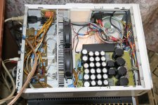
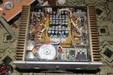
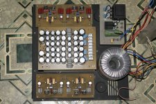
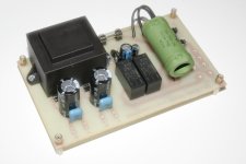
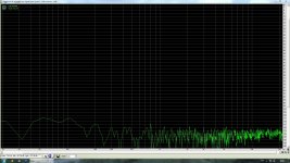
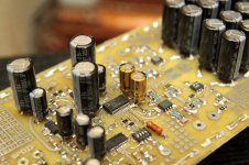
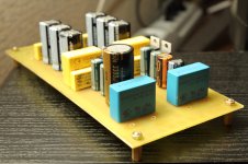
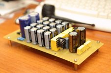
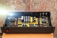
Le Classe 20W and Le Monstre schemes, max self noises le classe 20W and le monstre 8w, soft-start, Le Classe 20W for Rear Channels and Le Classe 30W for Center and Sub Channels, last photo - le monstre 8W test PCB. 🙂
Attachments
-
 _MG_2610.JPG598.6 KB · Views: 178
 -
 _MG_2587.JPG648.4 KB · Views: 185
 -
 _MG_2577.JPG666.9 KB · Views: 170
 -
 _MG_2560_ART.jpg634.9 KB · Views: 139
 -
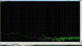 Le Classe 20W Own Noise Max.jpg433.3 KB · Views: 139
 -
 Le Monstre 8W EB2 2.JPG433.9 KB · Views: 328
 -
 Le Monstre 8W ART.jpg343.7 KB · Views: 348
 -
 20W_schematic ART Small.jpg654.6 KB · Views: 371
Last edited:
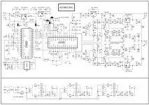
DAC will be not work on low impendance, 1 mA maximum output current. 10 mA bias can damage BJT (300 mW maximum).
what?? Are you talking about AD1853? It has a high impedance output. It needs an I/V stage, which is low impedance per definition. Look up the datasheet, and study the op amp output stages which are recommended. They have virtually 0Ohm input resistance at LF.
Your posted circuit might have about 5 to 10 ohms.
Re the bias...of course you have to chose the right transistors. 10mA would mean 30V over them for 300mW btw.........
Sorry, no, i do not have ready cooked circuits to offer for R2R.
I suggest you to play around, and learn this way. Read up on Jockos easy to build I/V, a more than 10 years old thread, good to learn the basics. Or the Pass D/A converter (D1?).
Hi,
the decision for a discrete IV stage, a openloop common-base in this instance, is a good one. 😉
The sound is regularly more authentic and more reallifelike.
Most OPamp stages sound technical to my ears.
Also as Sottomano states the lower the IVs input impedance and the more linear towards HF the better.
This is rather seldomly discussed here in the Forum and I assume that most apologets of OPamps simply don´t know about the input inpedance related issues.
Also the current through Vt4 and Vt5 defines input impedance.
The higher the lower the Zin.
Beeing a class-A stage the current must be higher than at least 1/2 of the DAC´s p-p output current.
But that´s theory ... in practise it requires at least 5 times the minimum value to keep THD low enough.
The circuit here could be twaeked in that You omit with Vt1, Vt2 and their emitter resistors and putting a resistor from each of the nodes Vt4/pin16 and Vt5/Pin13 to gnd (560R as start value).
This swill keep Vt4´s and Vt5´s emitter at the required Vref of 2.7V and allows for sufficient current (~5mA) through Vt4 and Vt5 to keep them safely in class-A.
If the heat power losses of Vt4 and Vt5 don´t suffice they may be replaced by a CFP stage, which also has the advantage of lowering the input impedance considerably.
Transistors Vt7 and Vt8 then also require the same measurements regarding their idle current.
Hence Resistors R29 and R32 need to be lowered to cope with the raised current values.
Routing Vt7 and Vt8´s current through these resistors is a nice way to do the balanced-to-SE conversion and it looks like a clever kind of THD-reduction at the same.
Other Tweaks that may reduce THD could be a change from the simple current mirror to a Wilson CM (adding just two transistors) and replacing the resistors R30, R31 by active current sources (just two additional transistors their Bases biased from VD6 and VD7).
The same applies to resistors R42 and R43 in the output buffers.
Another possible tweak could be to omit with the 2nd order output filter.
It seems that the AD1853´s output noise raises only >300kHz.
This renders a classical output filter obsolete and I´d replace it by 1st order RC-lowpass of 300-400kHz just to keep HF off of the following device.
Alternatively or additionally a small cap of a couple of pF between Vt4/Vt7´s emitters, resp. Vt5/Vt8´s emitters could remove possible glitch artefacts of the DAC and HF noise from entering the IV stage.
A last tweak regards the voltage regulators DA1, DA4 and DA6.
There are more modern lower noise regulators around.
The tweaks will lower numbers but will it improve sound?
Maybe, maybe not ... it´s not uncommon that the simplest circuits sound the most pleasant even if certain numbers look supsicious, yeah even ridicolous.
I´ve rather few doubts that the circuit has the potential to blow OPAmp stages off of their thrones with ease. 😉
I certainly like it 😀
jauu
Calvin
Hi,
the decision for a discrete IV stage, a openloop common-base in this instance, is a good one. 😉
The sound is regularly more authentic and more reallifelike.
Most OPamp stages sound technical to my ears.
Also as Sottomano states the lower the IVs input impedance and the more linear towards HF the better.
This is rather seldomly discussed here in the Forum and I assume that most apologets of OPamps simply don´t know about the input inpedance related issues.
Also the current through Vt4 and Vt5 defines input impedance.
The higher the lower the Zin.
Beeing a class-A stage the current must be higher than at least 1/2 of the DAC´s p-p output current.
But that´s theory ... in practise it requires at least 5 times the minimum value to keep THD low enough.
The circuit here could be twaeked in that You omit with Vt1, Vt2 and their emitter resistors and putting a resistor from each of the nodes Vt4/pin16 and Vt5/Pin13 to gnd (560R as start value).
This swill keep Vt4´s and Vt5´s emitter at the required Vref of 2.7V and allows for sufficient current (~5mA) through Vt4 and Vt5 to keep them safely in class-A.
If the heat power losses of Vt4 and Vt5 don´t suffice they may be replaced by a CFP stage, which also has the advantage of lowering the input impedance considerably.
Transistors Vt7 and Vt8 then also require the same measurements regarding their idle current.
Hence Resistors R29 and R32 need to be lowered to cope with the raised current values.
Routing Vt7 and Vt8´s current through these resistors is a nice way to do the balanced-to-SE conversion and it looks like a clever kind of THD-reduction at the same.
Other Tweaks that may reduce THD could be a change from the simple current mirror to a Wilson CM (adding just two transistors) and replacing the resistors R30, R31 by active current sources (just two additional transistors their Bases biased from VD6 and VD7).
The same applies to resistors R42 and R43 in the output buffers.
Another possible tweak could be to omit with the 2nd order output filter.
It seems that the AD1853´s output noise raises only >300kHz.
This renders a classical output filter obsolete and I´d replace it by 1st order RC-lowpass of 300-400kHz just to keep HF off of the following device.
Alternatively or additionally a small cap of a couple of pF between Vt4/Vt7´s emitters, resp. Vt5/Vt8´s emitters could remove possible glitch artefacts of the DAC and HF noise from entering the IV stage.
A last tweak regards the voltage regulators DA1, DA4 and DA6.
There are more modern lower noise regulators around.
The tweaks will lower numbers but will it improve sound?
Maybe, maybe not ... it´s not uncommon that the simplest circuits sound the most pleasant even if certain numbers look supsicious, yeah even ridicolous.
I´ve rather few doubts that the circuit has the potential to blow OPAmp stages off of their thrones with ease. 😉
I certainly like it 😀
jauu
Calvin
Guys, you absolutely confuse me...🙂
Hi,
Why?? 😉
Two older but still interesting papers regarding input impedance issues:
"Low Input Impedance Current-to-Voltage Conversion Circuit for Current-Output Digital-to-Analog Converters", Michael Smedegard, 101st AES Convention 1996, Nov 8-11th, LosAngeles
and
"Current Steering Transimpedance Ampifiers for High-Resolution Digital-To-Analog Converters", M.O.Hawksford, 109th AES Convention 2000, Sept. 22-25th, LosAngeles
Built the circuit from Fg.4-4 with error correction.
Unfortunately one of those examples where better figures due to higher complexity lead to inferior sonics compared to a simpler common-base stage like the Jocko and derivatives.
Hi,
Why?? 😉
Two older but still interesting papers regarding input impedance issues:
"Low Input Impedance Current-to-Voltage Conversion Circuit for Current-Output Digital-to-Analog Converters", Michael Smedegard, 101st AES Convention 1996, Nov 8-11th, LosAngeles
and
"Current Steering Transimpedance Ampifiers for High-Resolution Digital-To-Analog Converters", M.O.Hawksford, 109th AES Convention 2000, Sept. 22-25th, LosAngeles
Built the circuit from Fg.4-4 with error correction.
Unfortunately one of those examples where better figures due to higher complexity lead to inferior sonics compared to a simpler common-base stage like the Jocko and derivatives.
I'm amateur in DAC building. 🙄
This scheme in stock will have "normal/good" sound or not. 🙂
Thank for info, I'll try to find it on russian language.
Attachments
Hi,
Why?? 😉
Two older but still interesting papers regarding input impedance issues:
"Low Input Impedance Current-to-Voltage Conversion Circuit for Current-Output Digital-to-Analog Converters", Michael Smedegard, 101st AES Convention 1996, Nov 8-11th, LosAngeles
and
"Current Steering Transimpedance Ampifiers for High-Resolution Digital-To-Analog Converters", M.O.Hawksford, 109th AES Convention 2000, Sept. 22-25th, LosAngeles
Built the circuit from Fg.4-4 with error correction.
Unfortunately one of those examples where better figures due to higher complexity lead to inferior sonics compared to a simpler common-base stage like the Jocko and derivatives.
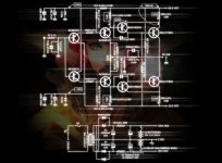
This scheme? (it's a little difficult for me)🙂
Attachments

it's a very good descret DAC schematics. It were made many veriants of this DAC with different USB modules like TE8802 XMOS CM6631A plus input selectors.
Sound is amazing - very soft and comfortable foe long tome listerning.
So I highly recommend to assemly!
Share my layout file with EPCOS output capacitors and recalculated output filter
Sound is amazing - very soft and comfortable foe long tome listerning.
So I highly recommend to assemly!
Share my layout file with EPCOS output capacitors and recalculated output filter
Attachments
Ad1862 is avaliable at rochester for 135 dollars : 2 units with shipment but without custims taxes...all others can be sourced on Ebay...but are they genuine ?
it's a very good descret DAC schematics. It were made many veriants of this DAC with different USB modules like TE8802 XMOS CM6631A plus input selectors.
Sound is amazing - very soft and comfortable foe long tome listerning.
So I highly recommend to assemly!
Share my layout file with EPCOS output capacitors and recalculated output filter
Thanx, but I've made AD1853 with classic output.🙂 Maybe I'll make discrete output later.😉
Attachments
it's a very good descret DAC schematics. It were made many veriants of this DAC with different USB modules like TE8802 XMOS CM6631A plus input selectors.
Sound is amazing - very soft and comfortable foe long tome listerning.
So I highly recommend to assemly!
Share my layout file with EPCOS output capacitors and recalculated output filter
sashok232,
Just came across this post. I downloaded your layout files, but the zip file appears to be corrupt because it cannot be opened in either Sprint Layout 6 nor Sprint Layout viewer.
Would appreciate if you could repost the layout files as I am interested to try out the ad1853 with a discreet i/v stage. Thanks
...The AD1853 is interesting but the AD1866 is pure R-2R I think, I prefer to support the pure R-2R, thermometer, string DAC's, not the Sigma-Delta, they are just cheaper to produce that's all...
Not only does it cost less, but sigma-delta, especially multi-bit sigma-delta, objectively performs better. Much better. Subjective sound, however, will vary as it is a matter of personal perception and preference.
- Status
- Not open for further replies.
- Home
- Source & Line
- Digital Line Level
- DAC AD1853 with discrete output