Another thing to consider, I'd try my best to put R5 and R8 as close as possible to the LM3x7 pins, instead of the protection diodes. Those diodes should have the least priority in position. Maybe this way you keep the ADJ lines shorter, to the 220uF coupling caps.
You should double check the LM3x7 pinouts. LM317 pinout is different from LM337 pinout.
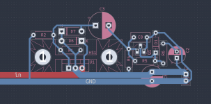
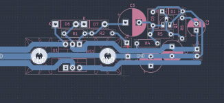
I made a quick draft of how I'd trace it. You can still keep the clean in/out/gnd trances by putting the input trace on the top side of the pcb.
I also used both protection diodes. (out-in and adj-out).
edit: actually your LM317 pinout is ok, you just have it rotated. Check the LM337 as well, you can simply use the input trace on the top side of the pcb to keep it tidy.
Attachments
Last edited:
Thanks again Trileru, I appreciate your comments.
Gilding the lily is the point of this exercise, I’ve learnt a lot about PCB layout doing this.
The PCB will be single sided, for home etching, otherwise I would use one of yours or the other excellent PCBs available. 🙂
Gilding the lily is the point of this exercise, I’ve learnt a lot about PCB layout doing this.
The PCB will be single sided, for home etching, otherwise I would use one of yours or the other excellent PCBs available. 🙂
Last edited:
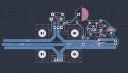
I actually like this kind of arrangement. Can be pretty thin this way. I cleaned the area around the protection diodes, moved the coupling cap a bit more inside etc. You get the idea. You'd still need a top wire but seems like a small price to pay.
Attachments
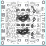
Tracking pre regulator LM317, LM337 with highly denoiser.
See WEB link below.
.
Using 3-pin regulators off-piste: part 4
.
See attached ZIP files.
PCAD2006 binary files.
Gerber files for China and Taiwan.
Dimension 100x100 mm.
.
You may use LM317HV, LM337HV .
VD7, VD12 is a LED with 2.8 ... 3.2 Volts across.
.
See WEB link below.
.
Using 3-pin regulators off-piste: part 4
.
See attached ZIP files.
PCAD2006 binary files.
Gerber files for China and Taiwan.
Dimension 100x100 mm.
.
You may use LM317HV, LM337HV .
VD7, VD12 is a LED with 2.8 ... 3.2 Volts across.
.
Attachments
Last edited:
A tracking pre-reg improves PSRR, but it does little for the output impedance, and nothing for the noise: you remain stuck with the noise spec of the basic 317/337
Tracking pre regulator LM317, LM337 with highly denoiser.
.
Why so many input capacitors?
Those need to be on the schematic, in order to match the numerous footprints placed in the PCB layout (for "Layout Versus Schematic" verification checks). The board assembler has the option to stuff and solder filter capacitors of widely varying diameters. See attachment 2 on post #2308
_
_
Attachments
Ah, I thought all were supposed to be installed. I didn't check the pcb design, looked only at the schematic. Makes more sense now.
sorry, not sure if it has been answered, i want to make a positive supply with output 7.5V-9V for my USB coax digital interface. it seems the denoise ( single transistor )version dose not work well below 11V. Will the two transistors one work well with or without mods? I simulated the single transistor version, and with the output at 7.5v or 12V, there is huge difference in performance.
At 7~9V, the standard, plain-vanilla denoiser should deliver its performance; maybe a bit lower than the typical 30dB improvement advertised for a 12V application but not far
Thanks Trileru , Elvee
My DC input is 13V and the load current is 0.5A
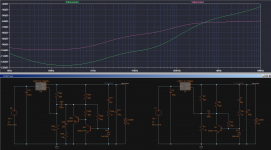
Looks to me that the big difference is when I run noise analysis , I got 14 nV total RMS at 10.8V output, but 164nV at 7.5V out. (1hz-100Khz)
The 620R, 62K resistor change makes some improvement but not big.
I use LT317A model from LTspice .
My DC input is 13V and the load current is 0.5A
Looks to me that the big difference is when I run noise analysis , I got 14 nV total RMS at 10.8V output, but 164nV at 7.5V out. (1hz-100Khz)
The 620R, 62K resistor change makes some improvement but not big.
I use LT317A model from LTspice .
Last edited:
If you are not going to use the LT317A in your circuit then maybe try the LM317 model from TI:
https://www.ti.com/product/LM317-N#design-tools-simulation
https://www.ti.com/product/LM317-N#design-tools-simulation
IIRC correctly, the LT317 model doesn't include noise which is why I modelled the improvement brought by the denoiser using an explicit voltage sourceThanks Trileru , Elvee
My DC input is 13V and the load current is 0.5A
Looks to me that the big difference is when I run noise analysis , I got 14 nV total RMS at 10.8V output, but 164nV at 7.5V out. (1hz-100Khz)
The 620R, 62K resistor change makes some improvement but not big.
I use LT317A model from LTspice .
Hi Trileru,I actually like this kind of arrangement. Can be pretty thin this way. I cleaned the area around the protection diodes, moved the coupling cap a bit more inside etc. You get the idea. You'd still need a top wire but seems like a small price to pay.
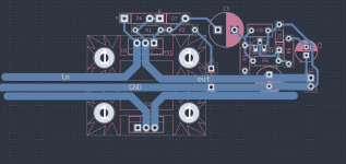
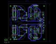
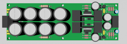
I have what I hope is the final version of the layout, based on the advice that you and the other here have so kindly given.
I've really enjoyed this as an intellectual exercise and have learned a lot about laying out a PCB from a schematic.
Having a power supply, the next step is to learn to lay out an op amp line level analogue circuit, probably a preamp or a active crossover.
I would be grateful if you wouldn't mind casting your eye over the PCB below as a sanity check to make sure I haven't connected something up incorrectly. I've tried to keep the loop areas small and take feedback from the right place as per your advice.
Attachments
- Home
- Amplifiers
- Power Supplies
- D-Noizator: a magic active noise canceller to retrofit & upgrade any 317-based VReg