Re: I'm sure you knew When he bit off more than he could chew.
😀
Where ignorance is bliss it most certainly is folly to be wise.
....i am done here....BYE! 😎
MalichiConstant said:I suggest you stop reading Cherry, and Smith, Koen, Witulski....... and learn Ohm's law and some simple basics about how a transistor works.
😀
Where ignorance is bliss it most certainly is folly to be wise.
....i am done here....BYE! 😎
Re: I'm sure you knew When he bit off more than he could chew.
Speak for yourself old chap....speak for yourself.... 😉
MalichiConstant said:I was a victim of a series of accidents, as are we all
Speak for yourself old chap....speak for yourself.... 😉
Ouroboros said:People forget that a bipolar transistor is actually a voltage controlled device, with a mathematically precise exponential Ic/Vb transfer function that holds over many decades.
Actually people like Malachiconstant DO NOT KNOW that a BJT is in fact a VCCS.....and sadly, probably never will...... 🙄
Mike,
.....................but what about the schematic UT requested, seems like a reasonable request.
Regards,
Jam
.....................but what about the schematic UT requested, seems like a reasonable request.
Regards,
Jam
Stick a fork in him........
"....i am done here....BYE!"
I think you were done a long time ago in this thread.
"....i am done here....BYE!"
I think you were done a long time ago in this thread.
andy_c said:If one's only agenda is determining the truth of a matter, then the issue of who is right is irrelevant. The only thing that matters is what is right. Human nature seems to make this ideal difficult to achieve in practice. I'm not there yet, but I like to think I at least try.
A good dose of common sense from andy_c for Malachiconstant....

mikeks said:
A good dose of common sense from andy_c for Malachiconstant....
that very advice goes both ways, mikeks.
Re: Re: Re: Re: Re: Re: Re: let us come to the point
http://kabuki.eecs.berkeley.edu/~abo/papers/240/240_report.pdf
Ultima Thule said:Mike,
Could you please show a schematic of such a transimpedance amplifier?
http://kabuki.eecs.berkeley.edu/~abo/papers/240/240_report.pdf
millwood said:
how about this:
a bjt is a current-controlled resistor........
No...more like a voltage controlled resistor...
millwood said:
........and a mosfet is a voltage-controlled resistor.
Close....
This is a current feedback-current subtraction amp
bjt cccs/vccs issue explained
Greetings all,
I wanted to respond four weeks ago, but work has been hectic. Let's start with this BJT CCVS/VCVS issue.
Any two-port circuit which inputs V and I, and outputs V and I can be described as possessing current gain, voltage gain, transconductance, and transresistance. Take a simple R-C low-pass circuit. The input enters the resistor, and the output is taken across the capacitor. Now add a load resistance across the capacitor (output). We have Vin, Iin, Vout, and Iout. Is this circuit best described as voltage-in-voltage-out (voltage gain), current-in-current-out (current gain), transconductance (voltage-in-current-out), or transresistance (current-in-current-out)? The best answer is "all of the above". With pure linear circuit elements, there is no need to attempt to define behavior in terms of "voltage-controlled" or "current-controlled". By virtue of the circuit's linearity, a 10% change in input voltage produces a 10% change in input current, output voltage, and output current. The same effect is incurred when the input current changes by 10%. With a linear network, the I-V graph is a straight line, so that it makes no difference if the input is voltage-driven vs. current-driven. Hence, it is foolish to argue if this R-C-R network is a "VCVS", "CCVS", etc.
With nonlinear circuit elements, things change. Since the I-V graphs of a diode, BJT, JFET, etc. are nonlinear, a 10% change in I does not necessarily effect a 10% change in V, and vice-versa. Regarding the BJT, let us use the common emitter configuration (CE) for illustration. The bjt here is "in the raw", that is no biasing networks, no emitter resistor, etc. We do need base and collector resistors. The inputs are Ib and Vbe (base current and base-emitter voltage resp.). The outputs are Ic and Vce (collector current and collector-emitter voltage resp.). We have four transfer functions, current gain Ic/Ib, transconductance Ic/Vbe, voltage gain Vce/Vbe, and transresistance Vce/Ib. The question here, which seems to get people worked up, is "Which transfer parameter most accurately describes the operation of a bjt?"
My answer would be "What are you trying to achieve? Are you building a logarithmic amp for data processing, or a linear amplifier with minimal distortion?" I hold a patent on a log amp and have worked with such amps for about a decade. Some have described the relation between Vbe and Ic (or Ib for that matter) as logarithmic over many decades. The problem is that the leakage or saturation curent, Is, varies exponentially with temperature. Using a 2N4401 npn bjt, for example, the saturation current is around 5 nanoamp at T = 25 deg C, but reaches 814 microamp at T = 125 C, an increase by a factor of 162,755. In addition the thermal voltage term in the equation, Vt ( = kT/q, where k is Boltzmann's constant, and q is unit charge on single electron) changes from 50 millivolt at 25 C to 67 millivolt at 125 C. In order to use the exponential junction characteristic of a bjt for log/antilog amp applications, or a diode for that matter, we must include two-step temperature compensation, both offset and slope correction. Without this compensation, the Vbe/Ic relation is grossly out of whack as temperature varies. With Vbe = 0.60 volt, Ib = 0.814 mA at 25 deg C. Increasing Vbe by 10% to 0.66 V, gives Ib = 2.702 mA. Increasing Vbe by 10% increased Ib to 332% of its original value. At 125 deg C, Vbe = 0.60 V gives Ib = 6.3 amp, and Vbe = 0.66 V gives 15.4 amp! If linear amplification is the objective, the Vbe/Ic relation will produce huge distortion due to its exponential characteristic which increases with temperature.
What about Ic vs. Ib, aka "hfe", or "beta". The Ic vs. Ib relation is not exactly linear, but we will see that it is much closer to linear than Ic/Vbe. At 25 C, let's start with 1.0 mA of base current. The collector current Ic, is hfe*Ib. With hfe nominally at 80, Ic = 80 mA. Increasing Ib by 10% gives roughly a 10% increase in Ic, or 88 mA. If Ib increases by a factor of 10, beta increases to about 150, and Ic is now 1.5 A. Increasing Ib by 10 increases Ic by almost 19. Some distortion is inevitable. At 125 C, beta increases by a factor of roughly two, so that the collector currents in the previous example double. Also worth mentioning is that signal beta, hfe, can reach as low as 40 min, and as high as 500 max, a variation factor of 12.5. Considering the doubling with temp, we have a variation of 25. Quite a lot, but still much less than if we drove Vbe trying to control Ic.
It is quite clear that beta is not as linear as we would like, and that the distortion resulting from beta dependency is substantial. Beta varies from one device to the next, with current level, and temperature. Fortunately, such variations can be minimized with biasing and emitter degeneration.
Also worth noting. Some web sites describe Ic as being directly related (caused) by Vbe, with Ib being a parasitic loss, or side-effect of Ic. When electrons flow through the p-n junction, a small fraction fail to recombine, and this is the base current, the loss, or "defect" quantity. For those who ascribe to this point of view, will you please answer the following loaded question:
If Ib is a only side-effect of Ic, why is it that if the collector is open circuited, Ic = 0, that Ib still flows with applied Vbe??? As the collector resistance is reduced from infinite down to a value consistent with active region operation, Ib hardly changes at all. Ib flows with or without Ic. Therefore Ib exists on its own, and cannot be caused by Ic. Ic, however, cannot exist without Ib (except for Iceo, the off state leakage current, very small).
Let's remember that the relation between Vbe and Ib is MUTUAL INCLUSION, not cause/effect. Ic, however is an effect of BOTH Vbe/Ib simultaneously. With Vbe and Ib, one cannot exist without the other. The two together can exist with or without Ic. Ic cannot exist without Ib/Vbe.
Also, some have stated on their web sites that beta is not a fundamental bjt quantity, because it varies too much from part to part. Based on that logic, transconductance gm then cannot be a fundamental JFET quantity because it also varies from part to part. With JFETs, transconductance IS a fundamental parameter. The fact that gm varies does not alter the fact that a JFET is a voltage controlled current source. With op-amps, open loop voltage gain is a fundamental property. This quantity also varies from one part to the next. Open loop gain is STILL a basic quantity, regardless.
Maybe this week, I'll present more examples of cfb error signal action. Bye.
Re: bjt cccs/vccs issue explained
The basic operation of a BJT does not conveniently change with application...
🙂
Claude Abraham said:The question here, which seems to get people worked up, is "Which transfer parameter most accurately describes the operation of a bjt?"
My answer would be "What are you trying to achieve?
The basic operation of a BJT does not conveniently change with application...
🙂
Re: Re: bjt cccs/vccs issue explained
IMHO
I don’t think that anyone said anything about changing the way the BJT works
The basic operation does not change, but the way you describe the function by means of math needs to be chosen with care. The linear small signal model only works when a small signal is applied (What levels are small can be discussed later) but needs to be revised and altered to a large signal model when the transistor is driven with large signals.
This is often the case when modelling real world systems. The model is made linear to be easier to handle, and because that type of model often is enough to achieve the needed results and learn what’s necessary about a system.
\Jens
Re: Re: Re: bjt cccs/vccs issue explained
The BJT will function as a VCCS regardless of the way it's driven....
Different allowances have to made of course for diiferent modes of operation, but the afore-mentioned basic fact remains unchanged..
JensRasmussen said:IMHO
I don’t think that anyone said anything about changing the way the BJT works
The BJT will function as a VCCS regardless of the way it's driven....
Different allowances have to made of course for diiferent modes of operation, but the afore-mentioned basic fact remains unchanged..
That a BJT is a current output device can be seen from the fact that the collector voltage depends on the collector resistor (to a first degree at least, nobody is perfect). If it was a voltage output device, the collector voltage would not vary with the collector resistor.
Jan Didden
Jan Didden
Re: Re: Re: Re: bjt cccs/vccs issue explained
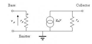
Can you elaborate this a bit more for us please, preferable with a picture of a VCCS model of a BJT?
Cheers 😉
mikeks said:
The BJT will function as a VCCS regardless of the way it's driven....
Can you elaborate this a bit more for us please, preferable with a picture of a VCCS model of a BJT?
Cheers 😉
Re: Re: Re: Re: Re: bjt cccs/vccs issue explained
Here you go: 🙂
Pjotr said:
Can you elaborate this a bit more for us please, preferable with a picture of a VCCS model of a BJT?
Cheers 😉
Here you go: 🙂
Attachments
- Status
- Not open for further replies.
- Home
- Amplifiers
- Solid State
- Current feedback - Voltage feedback, how do I see the difference?