...I do think it comes down to asking why the "other camp" believes that the existence of voltage feedback means that there can be no current feedback whatsoever.
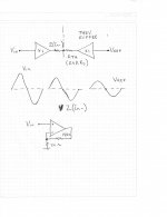
Attached is a visual representation of a thought I questioned some time ago. I added some sinusoidal waveforms to show that the Thevenin buffered output is always to degree smaller than Vin and whereupon V Z(In-) is of amplitude between them. The idea is that if V Z(In-) is of amplitude toward matching that of Vin than the CFA device is a c.f. amplifier, that alternatively the CFA device is a v.f. amplifier.
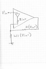
In the first approximation ( if this is possibly true ), a 10x feedback amplifier is shown whereupon the parallel combination of Rf||Rg is approx. 18 Ohms. Given that the CFA has a Z[In-] of perhaps 50 Ohms this suggests that it ought to be a v.f. amplifier if my thinking is correct. I wonder if you would check this out using Middlebrook before considering this further. I have no access to a simulator.
Attachments

@Chris
Thank you for looking at the Ro cancellation.
I will come back to your question tomorrow.
Hans
Thank you for looking at the Ro cancellation.
I will come back to your question tomorrow.
Hans
Attached is a visual representation of a thought I questioned some time ago. I added some sinusoidal waveforms to show that the Thevenin buffered output is always to degree smaller than Vin and whereupon V Z(In-) is of amplitude between them. The idea is that if V Z(In-) is of amplitude toward matching that of Vin than the CFA device is a c.f. amplifier, that alternatively the CFA device is a v.f. amplifier.
In the first approximation ( if this is possibly true ), a 10x feedback amplifier is shown whereupon the parallel combination of Rf||Rg is approx. 18 Ohms. Given that the CFA has a Z[In-] of perhaps 50 Ohms this suggests that it ought to be a v.f. amplifier if my thinking is correct. I wonder if you would check this out using Middlebrook before considering this further. I have no access to a simulator.
I'm not quite sure what the test is. I believe that whether we are talking about a standard CFA, a Thevenin equivalent CFA or a VFA , all in the non-inverting configuration, I'd always expect an excitation sine wave at In+ to be larger than that at In-.
Could you state what premise you'd like tested? I can run the sim for you.
Just so you know, LTSpice is freeware. If you have a computer, you can have a simulator at no additional cost.
Chris,HI Hans,
Some Questions:
Doesn’t this change the DC bias current and therefore gm?
Doesn’t this multiply all transistor currents by an AC signal which is a function of vce?
The only way I see to cancel vce/ro is if the term in the square brackets were zero, and it’s not. (And if it were, it would cancel everything!)
Wouldn’t a cancellation of the AC portion of the Early current be more appropriately accomplished by replacing the current source with a large capacitor in series with a negative resistance? LTSpice allows negative resistors.
I welcome your thoughts.
I had a few seconds time.
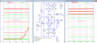
Does the image below, showing both the regular BC550C and the one compensated for Ro, already answer some of your questions ?
Hans
Attachments
Chris,
I had a few seconds time.
Does the image below, showing both the regular BC550C and the one compensated for Ro, already answer some of your questions ?
Hans
No, I'm afraid not.
Chris,
I had a few seconds time.
Does the image below, showing both the regular BC550C and the one compensated for Ro, already answer some of your questions ?
Hans
This simple approach accomplishes Early cancellation with no AC intermodulation, no multiplicative effect on other currents, and with minimal DC bias shift. DC bias shift would be eliminated and AC Early cancellation maintained if the negative resistor were AC-coupled.
Attachments
I'm not quite sure what the test is. I believe that whether we are talking about a standard CFA, a Thevenin equivalent CFA or a VFA , all in the non-inverting configuration, I'd always expect an excitation sine wave at In+ to be larger than that at In-.
Could you state what premise you'd like tested? I can run the sim for you.
Thanks Paul.
My premise is based upon the assumption that the amplitude of the excitation sine wave across In+ and In- must be larger than across Rf || Rg in order for a CFA to become a v.f., hence it depends upon your expectation.
I simply wanted to know what Middlebrook predicts in using a standard CFA part that you might normally use from your library in a network comprised of Rf || Rg values less than Z(In-) as in the connection below. If the outcome identifies the device as a v.f. amplifier this indicates that a transition point must exist at some point whereupon a CFA becomes a c.f. or v.f. device, or visa versa.
If true, then the followup question becomes if the transition point is predictable. If so a simplistic model can exist as the basis of arguments for both camps as potentially to accept or reject the model. This might open lines of communication or reconsideration. However, this continuation begins with the question: Is it true that Middlebrook predicts a v.f. amplifier if configured with a low Rf || Rg? I may be completely wrong Paul.
I will look into the LTSpice thing... though it might be a long learning curve.
Attachments
Thanks Paul.
My premise is based upon the assumption that the amplitude of the excitation sine wave across In+ and In- must be larger than across Rf || Rg in order for a CFA to become a v.f., hence it depends upon your expectation.
I simply wanted to know what Middlebrook predicts in using a standard CFA part that you might normally use from your library in a network comprised of Rf || Rg values less than Z(In-) as in the connection below. If the outcome identifies the device as a v.f. amplifier this indicates that a transition point must exist at some point whereupon a CFA becomes a c.f. or v.f. device, or visa versa.
If true, then the followup question becomes if the transition point is predictable. If so a simplistic model can exist as the basis of arguments for both camps as potentially to accept or reject the model. This might open lines of communication or reconsideration. However, this continuation begins with the question: Is it true that Middlebrook predicts a v.f. amplifier if configured with a low Rf || Rg? I may be completely wrong Paul.
I will look into the LTSpice thing... though it might be a long learning curve.
Hierfi, my given name is Chris.
The analysis I did in my article shows that for adequate loop gain, to a good approximation, if the impedance seen by the inverting input looking into the feedback network is greater than the impedance Zin- seen looking into the inverting input, then Middlebrook will declare that c.f. predominates. Otherwise, v.f. does.
Suppose we assume a given value of Zin-. I'll simulate with an LT1395 CFA and measure Zin-. Please propose some values for Rg and Rf expressed in terms of Zin-. I assume you'll want an ideal unity gain buffer driven by the (unloaded) op amp output times Rg/ (Rg + Rf). Rg || Rf will connect the buffer output to the inverting input. You are interested in seeing (In+) - (In-), and the voltage across Rg || Rf, correct?
Sorry... Sometimes when I concentrate heavily on one thing my mind stops functioning altogether on things unquestionably known.Hierfi, my given name is Chris.
If the impedance seen by the inverting input looking into the feedback network is greater than the impedance Zin- seen looking into the inverting input, then Middlebrook will declare that c.f. predominates. Otherwise, v.f. does.
This follows my line of thinking from the Thevenin translation as well.
Suppose we assume a given value of Zin-. I'll simulate with an LT1395 CFA and measure Zin-. Please propose some values for Rg and Rf expressed in terms of Zin-.
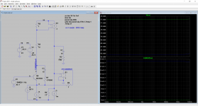
Sure. The attached figure identifies Rg and Rf in a relationship to Zin- with an arbitrary 10x gain. It is in using the LT1395 with the simulator measured values of Zin- in conjunction with values of Rg and Rf expressed in terms of Zin- that I would like you to use in a Middlebrook examination. I wanted to compare your results with my interpretation in using the Thevenin translation as identifying this as the crossover point of a CFA being a v.f. or c.f. device.
[/QUOTE]
Attachments
Hans
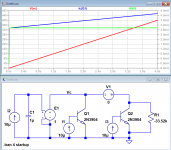
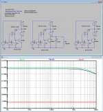
Gents, In the attached, it can be seen that the connection of AC-coupled negative value resistors between the emitter and collector of the inverting input transistors has a big effect on the range of ic6/vbe6 as Rload varies.
The range goes from 300:1 to 3:1!
Although this Early or Early-like effect may not be the only explanation for the 300:1 variation in the uncompensated circuit, it does appear to be the major one.
Attachments
Gents, In the attached, it can be seen that the connection of AC-coupled negative value resistors between the emitter and collector of the inverting input transistors has a big effect on the range of ic6/vbe6 as Rload varies.
The range goes from 300:1 to 3:1!
Although this Early or Early-like effect may not be the only explanation for the 300:1 variation in the uncompensated circuit, it does appear to be the major one.
Chris,
I did the same on a single input device with the same cancellation method.
When the impedance load is the opposite of cancellation res, ic/vbe goes down to ~0.....
Attachments
Chris,
I did the same on a single input device with the same cancellation method.
When the impedance load is the opposite of cancellation res, ic/vbe goes down to ~0.....
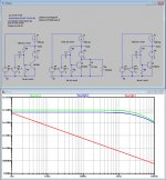
Herve, our results are quite different. In my case, the introduction of the negative resistors reduces the range of variation of ic/vbe from 300:1 to 3:1. It also shows that whether the resistors are there or not, vbe varies more or less inversely with loop gain as might be expected, as less collector current is needed to close the loop with higher gains.
The lack of vbe variations in your results contradicts my intuition of how this circuit should work. There should be roughly an inverse relationship between vbe and loop gain until the Early or Early-like effect kicks in. Do you agree? I welcome your comments.
Chris,
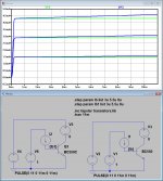
What about this attempt to show you the effect of Ro cancellation.
I have made a simple one transistor model with a current source in the collector, where gain is restricted by Ro, so cancelling Ro should result in a higher loop gain.
The exact same amount of current as in our complete model and also the same Vce of 22.8V DC has been set.
Left is my BC550 model with Dynamic ro cancellation as used before, but now also with an added negative cap to cancel the cap par. to ro.
Middle version is with the BC550C model, but now a negative resistor and a negative cap in par. to achieve te same cancellation.
Difference between the two is resp AC and DC cancelation for ro and R0, but as you can see, the difference is not that relevant.
The model to the right is without any cancellation, showing an open loop gain that is significantly smaller because of Ro.
Hans
Attachments
Herve, our results are quite different. In my case, the introduction of the negative resistors reduces the range of variation of ic/vbe from 300:1 to 3:1. It also shows that whether the resistors are there or not, vbe varies more or less inversely with loop gain as might be expected, as less collector current is needed to close the loop with higher gains.
The lack of vbe variations in your results contradicts my intuition of how this circuit should work. There should be roughly an inverse relationship between vbe and loop gain until the Early or Early-like effect kicks in. Do you agree? I welcome your comments.
Of course I agree, but I don't see my results contradict that.
Here are results with almost the same scheme as your.
You can see that for RLOAD = 250kohm (R cancellation/2) ic/vbe is also near 0.
This Ro cancellation is not devoid of collateral damage.
Attachments

You can turn off Early effect using
.model BC550C2 AKO:BC550C NPN Vaf=1g
Which makes a new model BC550C2 which is a copy of BC550C but with Vaf=1g.
.model BC550C2 AKO:BC550C NPN Vaf=1g
Which makes a new model BC550C2 which is a copy of BC550C but with Vaf=1g.
Chris,
What about this attempt to show you the effect of Ro cancellation.
I have made a simple one transistor model with a current source in the collector, where gain is restricted by Ro, so cancelling Ro should result in a higher loop gain.
The exact same amount of current as in our complete model and also the same Vce of 22.8V DC has been set.
Left is my BC550 model with Dynamic ro cancellation as used before, but now also with an added negative cap to cancel the cap par. to ro.
Middle version is with the BC550C model, but now a negative resistor and a negative cap in par. to achieve te same cancellation.
Difference between the two is resp AC and DC cancelation for ro and R0, but as you can see, the difference is not that relevant.
The model to the right is without any cancellation, showing an open loop gain that is significantly smaller because of Ro.
Hans
Hans, The model on the left still concerns me for the reasons I mentioned earlier. I am not confident that over a range of vbe levels it accomplishes the same results as the negative resistor does.
Additionally, post 2210 would seem to confirm that Early is responsible for almost all of the variation of ic/vbe from from gm = IC(DC)/ (kt / q) as loop gain varies. Do you agree?
You can turn off Early effect using
.model BC550C2 AKO:BC550C NPN Vaf=1g
Which makes a new model BC550C2 which is a copy of BC550C but with Vaf=1g.
Cool! Thanks!
When doing that, my third model at the right becomes like this.You can turn off Early effect using
.model BC550C2 AKO:BC550C NPN Vaf=1g
Which makes a new model BC550C2 which is a copy of BC550C but with Vaf=1g.
Is there also a parameter that can be changed to nihilate the cap par. to Ro ?
Hans
Attachments
- Home
- Amplifiers
- Solid State
- Current Feedback Amplifiers, not only a semantic problem?