Hi Elbert,
I would expect the servo to overload with your offset problem.
Nikos,
would you please check your amplifier and servo outputs? Have you got equipment or techniques to carry out this check?
I would expect the servo to overload with your offset problem.
Nikos,
would you please check your amplifier and servo outputs? Have you got equipment or techniques to carry out this check?

Elbert,
I need to add a few more comments. In my earlier post I said that the missing 1mA must be going into the base of T7. This is one of two possible problems. The other possibility is that there is a serious problem with T2 and you are losing this 1mA through the emitter of T2.
I think this is a remote possibility, but, it nevertheless is a possible issue.
I would focus on T7 first. If this proves to be ok, then take a careful look at T2.
I really hope you solve this problem in the next day or so.
Bonsai,
I really hope a solution materialises soon too ,and I can only be very gratefull for the continuing support I have received so far!
At least I've been able to do some more measurements, and this is what I found so far..
Voltage across the T7 emitter resistor R25 was, 0,431V, which translates in to 13,06 mA emitter current
Corresponding value for T9 was 12,15 mA.
This seems to correspond with the "missing" 1mA from T6 as per your reasoning. Is this sufficient to close out T2 as a possible culprit?
I allso measured the voltage across Collector-emitter for T7, and this was 2,55V
Vbe was 0,717
For T9, I measured a Vce of 2,58V and a Vbe of 0,681V.
So, for me, the question looks like this: Is a problem with T7 causing a higher base-current draw ,or is this induced by some other problem??😕
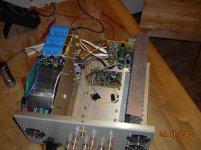
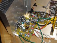
As per nikosokey's request and for general interrest, I've added a couple of pictures of one of the two amps I'm building. There will (eventually I hope!) be three channels in each chassis and an active X-over. 3-way active stereo is the plan.
The protection/ servo cards will be placed on the chassis floor, whilst the amplifier cards will be mounted on the large heatsink. Power-supply is a 2x38 VAC 600VA toroid feeding a double rectifier and 40000uF for each of the 3 channels.
I really hope a solution materialises soon too ,and I can only be very gratefull for the continuing support I have received so far!
At least I've been able to do some more measurements, and this is what I found so far..
Voltage across the T7 emitter resistor R25 was, 0,431V, which translates in to 13,06 mA emitter current
Corresponding value for T9 was 12,15 mA.
This seems to correspond with the "missing" 1mA from T6 as per your reasoning. Is this sufficient to close out T2 as a possible culprit?
I allso measured the voltage across Collector-emitter for T7, and this was 2,55V
Vbe was 0,717
For T9, I measured a Vce of 2,58V and a Vbe of 0,681V.
So, for me, the question looks like this: Is a problem with T7 causing a higher base-current draw ,or is this induced by some other problem??😕
As per nikosokey's request and for general interrest, I've added a couple of pictures of one of the two amps I'm building. There will (eventually I hope!) be three channels in each chassis and an active X-over. 3-way active stereo is the plan.
The protection/ servo cards will be placed on the chassis floor, whilst the amplifier cards will be mounted on the large heatsink. Power-supply is a 2x38 VAC 600VA toroid feeding a double rectifier and 40000uF for each of the 3 channels.
Attachments
Looks like you have spent a lot of money and effort there.
The transistors have alot of gain, and the Hfe can vary considerabley from device to device (though that normal inter device variability is not your problem here). Measuring the differences you see across the emitter resistors is within the normal range.
I can only see this problem at this stage coming from T7 or T2 - this is where the current must be 'leaking out'. If the currents comming out of T5 and T6 are equal (which they are at c. 3.7mA because you checked them), then they should add up across the LTP resistors and in your case they do not.
I would therefore at this stage try replacing T7 first and then if that shows no improvement, T2.
Last edited:
Well, Some effort perhaps, but not a huge deal of money, I've been very carefull about sourcing components and parts at good prices. Assumeing that I'm facing a semiconductor/ component quality issue here, the wisdom of that could perhaps be debated...
But despite having an "expendable income", one of the great satisfactions with DIY is to be able to build stuff that you would normally not afford.
Changing out T7 should be a small job, and I do happen to have one of these in spare..
BUT, it comes from the same batch (or at least bag) as the ones installed on the all the cards, so I need to take care and measure the transistors carefully here as there may not necessarily be a relative difference between the one on the card and its possible replacement!
I would be surprised if the problem was with T2, as this has allready been "replaced" as part of the matching I did. But then again, it seems evident that no door should be closed here untill the conclusion is made!
Check the pin out of the new T7, using the diode function of your DMM.
It will identify the base and whether PNP or NPN.
This method is not so good at differentiating collector from emitter.
If you have a transistor hFE tester then that should identify the collector vs emitter.
It will identify the base and whether PNP or NPN.
This method is not so good at differentiating collector from emitter.
If you have a transistor hFE tester then that should identify the collector vs emitter.
Good point from AndrewT - if you put a device in the wrong way around then you would also get this type of issue. Remember the other possible problem is T2. We are looking for the missing 1mA from the T6 constant current source - it can only be getting lost into T7's base, or in via T2's base.
BTW, what are the markings on the small signal transistors?
BTW, what are the markings on the small signal transistors?
I'll get the data-sheet for the T7 and look at the pin-out there: When I test the transistors, that should provide additional confirmation of correct pin-out.
The T7 transistor is marked thus:
CTBC
560C
Just plain letters, no logo or other distinguishing feature that might give a clue towards the origin or make of these transistors (same for the BC550C T9)
The T7 transistor is marked thus:
CTBC
560C
Just plain letters, no logo or other distinguishing feature that might give a clue towards the origin or make of these transistors (same for the BC550C T9)
CT is a code for the make
bc560c is the transistor type.
That last c is the hFE grade.
It should be CBE PNP.
i.e. diodes pass pointing into the base.
bc560c is the transistor type.
That last c is the hFE grade.
It should be CBE PNP.
i.e. diodes pass pointing into the base.
Yupp, that seems to agree with the data sheet I found!
Allthough it was a fairchild data-sheet, I guess it is stil valid.
Did a quick check on the one spare BC560C I have,
HFE was around 450, Base-current at 0,731V Vbe was around 1mA and that gave a collector current of 10mA.
I'll unsolder an check the transistor on the card, and I'll allso unsolder T9, BC550C and measure this one as well for comparison.
But what the...!!
Just unsoldered T7 from the card and popped it in to the Multimeter HFE tester..zero reading.. then I turned it arround the wrong way and it measures a Hfe of 250??!!
This indicates that the pin out is mirrored, and that Hfe is much lower than expected!? The transistor I unsoldered allso has a slightly different marking:
BC560C
K6B
Now, this transistor was either totally something else than it was supposed to be or it must have gotten damaged (?)
Only one thing to do now; solder in the spare BC560I had and fire the thing up!!
Which I just did, and the offsett was now around 0,6V as opposed to -8V previously.. So far so good!
Now, I'll hook up the servo and se what that does..
And so I did... offestt dropps from about 0,2V from start up.. crosses through zero.. and continues over to about -0,3V ?! (power off, quick!)
What could this be..?
I then remember that when adjusting the quiescent current previously, I had to turn the pot quite far on order to get the specified value.. but this setting might not be correct any longer now... best check that one and do it over again..
And right so, turned the pot all the way back and got the right quiescent setting with only a small nudge, not 2/3 turn.
But still the same behavior on the output offsett... Well, nobody said this was going to be easy..
Last edited:
Let me correct that last comment, it was easy, just had to connect the 0V power supply wire to the servo/ protection card...😱
Now I get an offset reading between 0 and 6mV (fluctuating a bit on the multimeter)
I'll bee sleeping well tonight!!🙂
Now I get an offset reading between 0 and 6mV (fluctuating a bit on the multimeter)
I'll bee sleeping well tonight!!🙂
Last edited:
Yes, finally success!
And what a relief that was, this certainly was frustrating, so It is very nice to get renewed hope of finishing the project! 🙂
So,
What have I learned from this?
First of all: Check all transistors before soldering together. Had I done so, I could have singled out that freak BC560 transistor even before I started building!
Second: Matching semiconductors is underrated, especially differential pairs.
Checking transistors and matching them can be done at the same time, so "two for the price of one" there.
I must extend a warm thanks to those who contributed to this thread Andrew, Wahab, Nikosokey, Leon, etc.. And last but not least Bonsai who managed to push me past the finishing line!
Thank you all for the support and the patience! 🙂
Now I need to complete the further assemblying and testing, something which will inevitably give throw up the odd obstacle here and there.
I might therefore continue to post on this thread every now and then, both to seek advice if necessary, but allso for general documentation for the benefit of anybody building the same amplifier in the future.
Now its time to tidy things up a bit and see if i can actually get some signals through the amplifier!
the reversed pin out of the rogue BC5xx is what a 2nxxxx is made to.
Better check all your stock.
Better check all your stock.
You bet I'll do Andrew! 🙂
Still don't get why that transistor was labeled BC560 though.. I have heard that there are bogus parts and counterfeits out there, but with a mirrored pin-out? Thats well blatant!
Just proves the importance of not taking things for granted...😡
Still don't get why that transistor was labeled BC560 though.. I have heard that there are bogus parts and counterfeits out there, but with a mirrored pin-out? Thats well blatant!
Just proves the importance of not taking things for granted...😡
Bonsai,
I'll definitively post some results when everything is assembled properly and running.
But due to the rather compact and convoluted layout of my design, it will probably take some time..
Anyway, thank you very, very much for your patience and kind assistance, you really saved the day!
Btw, a bit of topic, but what sort of loudspeakers do you use with your Ovation amplifier?
Hi Elbert,
I've got a pair of B&W 703's. If you google it you can get lots of reviews. They are a bit old now (IIRC launched in 2003) but they have agreat sound.
I've got a pair of B&W 703's. If you google it you can get lots of reviews. They are a bit old now (IIRC launched in 2003) but they have agreat sound.
- Status
- Not open for further replies.
- Home
- Amplifiers
- Solid State
- Crescendo Millennium offset problem