I think I spotted the problem.
Can you draw the schematic of the board as built and post it here?
Can you draw the schematic of the board as built and post it here?
i have checked till 1mhz with my scope seems ok , and i have 1/10X probes no issues there.. trying to find some 100X probes as i do work with a lot of switch-mode power-supplies...
So is my heatsink the issue , can i keep the current layout with the VBE placed on the main heat sink or do i need to modify and keep the VBE on a separate heat-sink with the driver.. ??
So is my heatsink the issue , can i keep the current layout with the VBE placed on the main heat sink or do i need to modify and keep the VBE on a separate heat-sink with the driver.. ??
I think I spotted the problem.
Can you draw the schematic of the board as built and post it here?
its the same as P3A amp no changes at all ....
its the same as P3A amp no changes at all ....
It looks like you are using 1943/5200 pairs.
Unmatched hFe in pairs of same could cause thermal runaway.
Why should the Vbe multiplier in a CFP OPS amp preferably be thermally connected to the CFP driver transistor instead of to any of the slave transistors (Q7, Q8)?
60-80W Power Amplifier
Hi Maiko, the quote from Douglas Self's web page:
"The CFP topology is generally considered to show better thermal stability than the EF, because the Vbe of the output devices is inside the local NFB loop, and only the driver Vbe affects the quiescent conditions. The true situation is rather more complex. [10],[11],[12]"
The references are:
10] Self, D "Thermal dynamics of Power Amplifiers: I" Electronics World, May 1996, p410.
11] Self,D "Thermal dynamics of Power Amplifiers: II" Electronics World, June 1996, p481.
12] Self,D "Thermal dynamics of Power Amplifiers: II" Electronics World, Oct 1996, p754.
It would be interesting to read the articles, however it's not easy to find Electronics World 1996 these days.
Cheers,
Valery
The pictures of the PCB are obscured but it appears that resistor R13 and R14 of P3A is missing - the collectors of the output transistors on your board appear to join up at the inductor node directly.mt490 ,
can you please point out what u think is the problem ?
The pictures of the PCB are obscured but it appears that resistor R13 and R14 of P3A is missing - the collectors of the output transistors on your board appear to join up at the inductor node directly.
yes the collectors are directly connected to the inductor as i have placed the resistor on the emitter .. cause i needed 2pairs of output devices
yes the collectors are directly connected to the inductor as i have placed the resistor on the emitter .. cause i needed 2pairs of output devices
Sekhar, that's the problem - with 2 pairs, you can add those resistors to the emitters, but you should not remove them from collectors.
The key for normal functioning of Vbe servo in CFP arrangement - having those resistors at the drivers' emitters - not the outputs' emitters. Resistors at the outputs' emitters will only help to better current distribution between the pairs.
Also, ones again - with CFP it's better to track the drivers' temperature, not the main heatsink's temperature. But you have to return the resistors back to the drivers' emitters.
Last edited:
Sekhar, that's the problem - with 2 pairs, you can add those resistors to the emitters, but you should not remove them from collectors.
The key for normal functioning of Vbe servo in CFP arrangement - having those resistors at the drivers' emitters - not the outputs' emitters. Resistors at the outputs' emitters will only help to better current distribution between the pairs.
Also, ones again - with CFP it's better to track the drivers' temperature, not the main heatsink's temperature. But you have to return the resistors back to the drivers' emitters.
Seems i have done a big mix up .....
this is how the output stage looks right now ....
Attachments

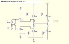
No 🙂 Collectors of the output transistors are both connected to the driver's emitter, connected to the resistor, going to the output.
In addition to that, you add a resistor to each emitter of the output transistor for better current distribution.
Cheers,
Valery
In addition to that, you add a resistor to each emitter of the output transistor for better current distribution.
Cheers,
Valery
Also, the base stoppers at the bases of the output transistors are not required in this arrangement.
some thing like this this is out of D .Self book ...No 🙂 Collectors of the output transistors are both connected to the driver's emitter, connected to the resistor, going to the output.
In addition to that, you add a resistor to each emitter of the output transistor for better current distribution.
Cheers,
Valery
Attachments
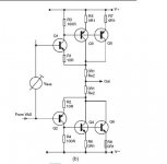
some thing like this this is out of D .Self book ...
Exactly - that's the right one.
Exactly - that's the right one.
thanks a lot , i will try out this configuration and report back....
its the same as P3A amp no changes at all ....
...but you did make a big change - you are using 2 pairs of output devices instead of 1. With a CFP output stage, you cannot simply parallel devices as you would with an EF stage.
AS others have commented, if you do not have 0.1 ohm current sharing resistors in the collectors for each transistor, in ADDITION to the 0.33 ohm emitter resistor, you will get thermal runaway.
Why do you need the extra pair of transistors anyway ? Are you using more than the recommended 35V supplies ? Are your 2SA1943/2SC5200's not genuine?
2Sc5200 is genuine no issues there .... I am going to use this amp from a subwoofer , and I needed 150W so using supplies of 42V , as my subwoofer is already 4E so could use the actual p3A as is ....
This is a misunderstanding that you seem to have missed in earlier posts. The Vbe multiplier in a CFP amplifier design like P3A (Q9) should thermally track the driver transistors, not the output devices nor should it be attached to or near their heatsink. If you simply look at the pic of the assembled P3A on the ESP website, you can see that the Vbe multiplier is attached (by cable-tie actually) to one of the driver transistors, so that is clearly what was intended..... i have tried using a bias of 10ma the bias drift definitely slows down a lot as compared to 75ma.. but isnt it the work of the VBE transistor to track the temperature rise in the heatsink and adjust the bias accordingly....
60-80W Power Amplifier
I am unsure what the effect of using SMDs for the drivers will be when located so close to the heatsink as well, but the same principle applies and I suggest using a through-hole part, just bent over one driver and in close proximity if not firm contact. As your PCB is not really suitable, it brings the drivers and Q9 close to the influence of heatsink and output devices so there is already a problem there that you may have to resolve with a new layout.
For reference, See Douglas Self's article on CFP biasing design (it's also in several editions of the handbook and "Self on Audio" books) for about the best description I've seen.
- Status
- Not open for further replies.
- Home
- Amplifiers
- Solid State
- Correct location for VBE bias transistor on CFP output amplifier