Hi, Steven,
Thanks for the info. With the properties of Q1, maybe this will work better than diamond buffer 😀
Thanks for the info. With the properties of Q1, maybe this will work better than diamond buffer 😀
Steven said
I am very curious about how a complimentary version would look like.
I understand your concern with the circuit working. I would think it might suffer from latch-up at turn on.
I did the circuit with mosfets. It seems to work. I don't how accurate the models I use are. I played around with transistors and it sometimes worked. I used caps across the c-b output transisitors for compensation to get the circuit stable when using transistors.
It gets tweaky using a simulator.
Tom
Attachments

Steven-
"Stasis comes from Greek and means "a standing still", see http://dictionary.reference.com/wor...2002/08/04.html"
i have a Stasi, one hell of a stasis, renamed basis from
Bill Gate's "Basic" just kidding, i dont see any stasis any more
just Basis all great things come from
cheers
"Stasis comes from Greek and means "a standing still", see http://dictionary.reference.com/wor...2002/08/04.html"
i have a Stasi, one hell of a stasis, renamed basis from
Bill Gate's "Basic" just kidding, i dont see any stasis any more
just Basis all great things come from
cheers
if i were a rich man ... yibber, deedle , didle, dum... if i were a biddy, biddy, rich... Mexican philanderer!
lot to do with audio..
lot to do with audio..
When exploring more linear input stages than standard differentials Gérard Perrot (Lavardin) became aware by some IC designers that there exists a "bipolar enhanced emitter follower" which was commonly used in IC's : both input (controling device) and output (controlled device) transistors are of the same polarity. It should have a lot less temperature drift than a CFP. In a CFP when current in the input device becomes larger, the current in the output device becomes larger, too.
This is the contrary in the enhanced follower which is very similar to the circuit shown by TOM2 with a few more elements to correctly polarise the bipolar junction transistors. The snag is that a CFP uses only two transistors and an enhanced follower uses three active devices, at least. However the circuit shown by Perrot has a slighly larger bandwidth than a CFP, probably due to a higher current in the input transistor.
~~~~~~~~~ Forr
§§§
Hi, TOM2,
Very nice 😀. Are they practically implementable in real output stage?
Hi, FORR,
Where can I see the schematic concept of Lavardin?
Very nice 😀. Are they practically implementable in real output stage?
Hi, FORR,
Where can I see the schematic concept of Lavardin?
lumanauw said
Are they practically implementable in real output stage?
I think the circuits are possible. Need to pay attention to compensation and possibly latch-up.
And of course getting the infamous power fet.
Tom
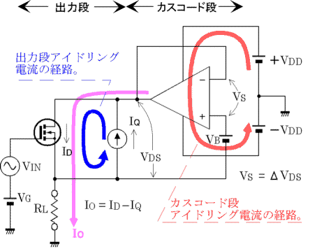
My idea for the moment is to have a low voltage psu with floating ground driven by a classAB amp ( Instead of the cascode ).
That would provide the constant voltage both for gain device and CCS.
Without that, the constant power topo looks like a big room heater to me.
That would provide the constant voltage both for gain device and CCS.
Without that, the constant power topo looks like a big room heater to me.
Got another ( real sick 😀 ) idea to not only get rid of the large current swings but also of the large currents...
Bernhard said:My idea for the moment is to have a low voltage psu with floating ground driven by a classAB amp ( Instead of the cascode ).
That would provide the constant voltage both for gain device and CCS.
Without that, the constant power topo looks like a big room heater to me.
Hi Bernhard,
Something like this?
http://www.ne.jp/asahi/evo/amp/2sk1380/report.htm
This circuit is from Shinichi Kamijo. Your idea triggered my memory about this amplifier. Actually it looks a lot like the circuit I proposed, but instead of the folded cascode and current source, he uses a floating low power supply voltage, which allows for a different way to force a constant current through the output FET (the 2SK1380). Looking at Kamijo's website, I think he is one of the most innovative amplifier designers, and a very productive one too.
Steven
Attachments
Tom2 said:
I understand your concern with the circuit working. I would think it might suffer from latch-up at turn on.
I did the circuit with mosfets. It seems to work. I don't how accurate the models I use are. I played around with transistors and it sometimes worked. I used caps across the c-b output transisitors for compensation to get the circuit stable when using transistors.
It gets tweaky using a simulator.
Tom
Hi Tom,
Exactly the same circuit topology I had put on paper, only with BJTs. But I had strong doubts about the (DC) stability, so I set it aside. In your circuit M5 and M6 will fight against each other, and instead of just forcing a current through M1 and M2, just as easy a big (almost uncontrolled) current will flow from M5 to M6 (cross conductance).
The Lovoltech power JFET is indeed a nice candidate for a Constans amplifier. It can handle big currents but its voltage rating is limited. The folded cascode takes care of that. BTW A group buy is going on in the Pass Labs forum for such a device.
Steven
Steven said:Hi Michael,
Your Q3 sees big voltage variations and dissipation (temperature) modulation. I know, a floating cascode, connected to the output can solve that, but then your circuit uses as many transistors as mine.
Another advantage of my circuit could be that the current in my output transistor is much larger. Any imperfect current modulation of Q2 (distortion) causes only a small percentage change in current of Q1, so the Vbe of Q1 will be very stable.
In your circuit, imperfections in the current dumper Q2 will cause more fluctuation in the collector current of Q3 and thus more Vbe changes.
Steven
Hi all,
been away during the weekend so I had to catch up all new posts.
But Steven, all that applies to your circuit too, no? 🙁
Not following you about where to put a cascode in my circuit, however:
The last sentence in your answer, my believe is that Q2 have the same early effect variations, eg. varying need of base current putting the same current modulation needs on both's Q3's which means both circuit's sink's away modulated currents through Q2 base and R1.
As a side note, you have probably noticed I purpously named Q2, Q3 and R1 in the same place as in your circuit just so it would been easier to discuss and compare each others circuits because they are doing the same thing here, eg. seeing same currents and voltages(except for a slight difference in Vce of Q3 in my circuit that sit's 0,65 V below), if all else equal.
But if I try to think about the currents going though Q1 I would interpret it like this way:
If we look at Q2 (especially with no emitter resistor) the Early effect will be very distinctive, said that what happens if we have high output voltage, this gives a decrease of the base current in most BJT's for a given current (which in our exercise is 2A 🙂 ), for low output voltage we have the opposite.
Now let's look at Q3 in your circuit, it's kind of shunting current passing by Q1 from Q3's emitter to base, but that's not much to talk about, however it shunts away current from emitter to collector by times hfe meaning there will for sure now not be any constant current through Q1, moreover the current modulation of Q3's base current needs also a small Vbe modulation meaning that the voltage is also not constant over Q1.
It's just thought through in my head so I can not be be fully sure but I guess you should see in your simulations something equal, for instance high output voltage = higher current through Q1(Q3 shunting less), and the opposite.
All this is in small quantities of course, but never the less I feel that Q1 is a "peace of dead meat", else if: 😀
I'm not sure I have yet grasped what is the main advantage with a circuit like yours(Q1), is it the constant base current need seen from the source (by means of fairly constant U/I over Q1 of course) that makes it more linear, or a bit something else?
If the main advantage is a more constant base current seen by the source then I could understand that might be the advantage, then, dose it have any merit's in reality?
But, on the other side, hope no one think I'm dissing, I do think this is an interesting discussion and brain exericse never the less! 🙂
Cheers Michael
Hi Steven,
thanks, good link...
This looks like what I would call parallel current injection, but not sure...
Is it possible to display that website in english ?
thanks, good link...
This looks like what I would call parallel current injection, but not sure...
Is it possible to display that website in english ?
Hi Bernhard,
Try Altavista: http://babelfish.altavista.com/
Select translation from Japanese to English. It works. Regretfully it does not work from Japanese to German...
Alex
Try Altavista: http://babelfish.altavista.com/
Select translation from Japanese to English. It works. Regretfully it does not work from Japanese to German...
Alex
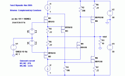
My schematic, not final 😉
30Vpp into 8 ohm load.
Idle power consumption 30W.
Output Fet idle current 2A.
Output FET ds voltage swing 300mV, ds current swing 50mApp @ full load.
Current source swing 3300mApp.

edit: R11, R17 = 100ohm.
30Vpp into 8 ohm load.
Idle power consumption 30W.
Output Fet idle current 2A.
Output FET ds voltage swing 300mV, ds current swing 50mApp @ full load.
Current source swing 3300mApp.
edit: R11, R17 = 100ohm.
Gerard Perrot
Hi Forr,
Where do you find these info on Gerard Perrot.s circuit?
Thanks
Sorry Bernhard for this interruption...
Hi Forr,
Where do you find these info on Gerard Perrot.s circuit?
Thanks
Sorry Bernhard for this interruption...
HI FAB
"Where do you find these info on Gerard Perrot.s circuit?"
In the french magazine "L'Audiophile" n°43, 1st trim 1988.
In his articles, Perrot studied some kinds of differential input
stages looking for high linearity (see his patent for the
finally chosen one) and then good subjective rendition
with a phono cartridge input !
~~~~~~~~ Forr
§§§
forr said:HI FAB
"Where do you find these info on Gerard Perrot.s circuit?"
In the french magazine "L'Audiophile" n°43, 1st trim 1988.
In his articles, Perrot studied some kinds of differential input
stages looking for high linearity (see his patent for the
finally chosen one) and then good subjective rendition
with a phono cartridge input !
~~~~~~~~ Forr
§§§
Hi Forr,
Thanks for the info!
Yes I have already a copy of the patents. So it means that the circuit you have provided is an earlier version. I used one in its patent (for my own personal use). Anyway, the amp input circuit in the Perrot patent is also used in Halcro patent.
- Status
- Not open for further replies.
- Home
- Amplifiers
- Solid State
- const. voltage & const. current on output FET ?