Re: Re: Re: Re: Stasis^2
Yes.
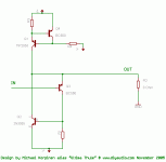
See patent 4,107,619 from Nelson Pass. In practice the amplifiers didn't have use an amplkifer 59 in fig 2 of that patent, but a Sziklai output stage. See circuit below.
Steven
Bernhard said:
The driver is the output ? Means Stasis output = constant current and constant voltage ?
Yes.
See patent 4,107,619 from Nelson Pass. In practice the amplifiers didn't have use an amplkifer 59 in fig 2 of that patent, but a Sziklai output stage. See circuit below.
Steven
Attachments
Hi Michael,
You've noticed it! There is a lot of similarity between my circuit and a CFP or Sziklai pair. Actually, my piece of scratch paper where I put the circuit on also contains your alternative circuit, only upside down, with NPN follower and PNP current dumper. Principally, this is the same circuit that is used in the Stasis amplifiers from Nelson Pass.
Only the CFP/Sziklai does not have a constant voltage across the transistor that determines the output voltage. Your Q3 sees big voltage variations and dissipation (temperature) modulation. I know, a floating cascode, connected to the output can solve that, but then your circuit uses as many transistors as mine.
Another advantage of my circuit could be that the current in my output transistor is much larger. Any imperfect current modulation of Q2 (distortion) causes only a small percentage change in current of Q1, so the Vbe of Q1 will be very stable.
In your circuit, imperfections in the current dumper Q2 will cause more fluctuation in the collector current of Q3 and thus more Vbe changes.
Steven
Very nice, Steven
You've created local current feedback around output transistor, two common base stages in loop path are potentially problemous at several MHz, did you think about freq. compensation?
You've created local current feedback around output transistor, two common base stages in loop path are potentially problemous at several MHz, did you think about freq. compensation?
Hi, Ultima Thule,
It is interesting that different people can interprete the same schematic (Steven's Constants) in a different view 😀
At first look, my view is like this :
The first thing is from Steven's explenation. No doubt that what happens with Q1 is very clever indeed.
I saw that current from IS1 (2A) is making 2 paths, one path is to collector of Q1, the other path is to emitor of Q3 (thus going to R1, activates base of Q2).
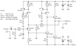
I saw this kind of action in JLH. In the attachment below, the CCS is Q8. It has 2 paths also, it can go to collector of Q3 (thus going to R9, activates Q1) or it can go to base of Q2.
But JLH doesn't have the constant I+V like Q1 in Steven's Constants.
Hi, Steven,
Am I wrong to interprete your Constants like above explenation? If IS1 in your Constants is 2A, then R1 value is the same as Q2's VBE voltage drop? (If Q2's VBE drop is 0V68, then R1=0R68?)
It is interesting that different people can interprete the same schematic (Steven's Constants) in a different view 😀
At first look, my view is like this :
The first thing is from Steven's explenation. No doubt that what happens with Q1 is very clever indeed.
I saw that current from IS1 (2A) is making 2 paths, one path is to collector of Q1, the other path is to emitor of Q3 (thus going to R1, activates base of Q2).
I saw this kind of action in JLH. In the attachment below, the CCS is Q8. It has 2 paths also, it can go to collector of Q3 (thus going to R9, activates Q1) or it can go to base of Q2.
But JLH doesn't have the constant I+V like Q1 in Steven's Constants.
Hi, Steven,
Am I wrong to interprete your Constants like above explenation? If IS1 in your Constants is 2A, then R1 value is the same as Q2's VBE voltage drop? (If Q2's VBE drop is 0V68, then R1=0R68?)
Attachments
Steven,
Great circuit. I like the reflected cascode and using the output
voltage as the base voltage for Q3. The complementary version
is also interesting to play with.
Tom
Great circuit. I like the reflected cascode and using the output
voltage as the base voltage for Q3. The complementary version
is also interesting to play with.
Tom
Not precisely a constant voltage constant current configuration (I suggest you see the Perrot - Lavardin patent where an input device having these features controls an output device in a feedback loop) but an interresting and almost unknown amp configuration : the Taylor's class B amp.
~~~~~~~~~Forr
§§§
~~~~~~~~~Forr
§§§
Attachments
I kindly like to remind on my basic question 🙂
Bernhard said:Would const. voltage Vds & const. current Ids on output FET reduce nonlinearity ?
Hi, Bernhard,
I'm not an expert here. But I think you will not be able to change the linearity of any device (bipolars, jfet, mosfet) by making constant current or constant voltage condition. They are what nature give, cannot be changed. What you can reduce by that 2 method is the distortion generated, it will be reduced. Like in bipolars, if you have the VCE constant, you will get minimum Early effect. Have you read the Peufeu "Memory Distortion"?
I'm not an expert here. But I think you will not be able to change the linearity of any device (bipolars, jfet, mosfet) by making constant current or constant voltage condition. They are what nature give, cannot be changed. What you can reduce by that 2 method is the distortion generated, it will be reduced. Like in bipolars, if you have the VCE constant, you will get minimum Early effect. Have you read the Peufeu "Memory Distortion"?
Bernhard,
If you really keep both Vds and Id constant, the whole question of linear of non-linear is pointless, since there is no change. Since you probably want to amplify or buffer with the device, you will have to use additional circuitry, for instance Stevens circuit. Then you will no longer keep Vds and Id perfectly constant. There will be som change to these parameters, and as Luamanuw said, you can't get away from the inherent non-linearities in the device. Howver, if you can keep the changes small and let the other circuitry do the job, you will get better linearity in this device, since both BJTs and FETs are more linear the smaller the change is, compared to the bias current. You might thus get a near-linear behaviour if you can keep the changes very small. On the other hand, some other device must now do the hard work and the non-linearities will show up in this device instead. Local feedback, as in a CFP, might reduce that non-linearity. It is not obvious you will get a better overall performance though. If we take a CFP, for instance, it will have lower distorsion than an emitter follower with the same bias current, but the spectrum will not fall off as quickly, so the high-order distorsion will be more prominent.
If you really keep both Vds and Id constant, the whole question of linear of non-linear is pointless, since there is no change. Since you probably want to amplify or buffer with the device, you will have to use additional circuitry, for instance Stevens circuit. Then you will no longer keep Vds and Id perfectly constant. There will be som change to these parameters, and as Luamanuw said, you can't get away from the inherent non-linearities in the device. Howver, if you can keep the changes small and let the other circuitry do the job, you will get better linearity in this device, since both BJTs and FETs are more linear the smaller the change is, compared to the bias current. You might thus get a near-linear behaviour if you can keep the changes very small. On the other hand, some other device must now do the hard work and the non-linearities will show up in this device instead. Local feedback, as in a CFP, might reduce that non-linearity. It is not obvious you will get a better overall performance though. If we take a CFP, for instance, it will have lower distorsion than an emitter follower with the same bias current, but the spectrum will not fall off as quickly, so the high-order distorsion will be more prominent.
Christer said:Howver, if you can keep the changes small and let the other circuitry do the job, you will get better linearity in this device, since both BJTs and FETs are more linear the smaller the change is, compared to the bias current. You might thus get a near-linear behaviour if you can keep the changes very small.
This is what I hoped to hear.
Christer said:
On the other hand, some other device must now do the hard work and the non-linearities will show up in this device instead.
But is this important ? If the circuit is SE, the CVC ( constant voltage & current ) gain device determines the output voltage.
The modulated current source just sinks current.
So far I remember Nelson Pass stated, the CCS does not deliver voltage, only current which is the advantage of SE classA over PP classA.
Christer said:Local feedback, as in a CFP, might reduce that non-linearity. It is not obvious you will get a better overall performance though. If we take a CFP, for instance, it will have lower distorsion than an emitter follower with the same bias current, but the spectrum will not fall off as quickly, so the high-order distorsion will be more prominent.
What is CFP ?
Bernhard said:
What is CFP ?
Also called a Sziklay pair.
EDIT:
Forgot this.
But is this important ? If the circuit is SE, the CVC ( constant voltage & current ) gain device determines the output voltage.
The modulated current source just sinks current.
So far I remember Nelson Pass stated, the CCS does not deliver voltage, only current which is the advantage of SE classA over PP classA.
This is not quite true, since the distorsion is a function of the whole circuit.
darkfenriz said:Very nice, Steven
You've created local current feedback around output transistor, two common base stages in loop path are potentially problemous at several MHz, did you think about freq. compensation?
No, I have not thought about frequency compensation (yet). I think this will be solvable, but it was just a paper idea and the sim worked instantly 🙂 .
Loop gain can be low. There is no need for high loop gain with virtually no current modulation in the output transistor Q1. A lower loopgain makes the current compensation via Q2 less perfect, so there is still some current modulation in Q1 left which causes some distortion, but it is still better than no compensation at all. No compensation is equivalent to just an emitter follower and emitter followers are used very often, also in amplifiers without overall feedback.
Steven
lumanauw said:
At first look, my view is like this :
The first thing is from Steven's explenation. No doubt that what happens with Q1 is very clever indeed.
I saw that current from IS1 (2A) is making 2 paths, one path is to collector of Q1, the other path is to emitor of Q3 (thus going to R1, activates base of Q2).
I saw this kind of action in JLH. In the attachment below, the CCS is Q8. It has 2 paths also, it can go to collector of Q3 (thus going to R9, activates Q1) or it can go to base of Q2.
But JLH doesn't have the constant I+V like Q1 in Steven's Constants.
Hi, Steven,
Am I wrong to interprete your Constants like above explenation? If IS1 in your Constants is 2A, then R1 value is the same as Q2's VBE voltage drop? (If Q2's VBE drop is 0V68, then R1=0R68?)
Hi Lumanauw,
I don't think the circuit is comparable to JLH's circuit, where in that circuit Q3 is used as phase splitter. As far as I see the resemblance of two different current paths is irrelevant and for different functions.
In my circuit, do not make R1 that low (0.68 Ohm). In fact, in the simulation it was 100 Ohm. You can even leave it out, neglecting HF behavior. Low values of R1 make the loop gain of the current compensator very low, causing imperfect cancellation.
Steven
Tom2 said:Steven,
Great circuit. I like the reflected cascode and using the output
voltage as the base voltage for Q3. The complementary version
is also interesting to play with.
Tom
Hi Tom,
Thank you. I am very curious about how a complimentary version would look like. It cannot be a simple mirroring, making a single ended output push-pull. The current dumpers or current compensators would fight against each other.
Steven
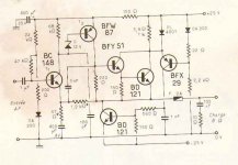
forr said:Not precisely a constant voltage constant current configuration (I suggest you see the Perrot - Lavardin patent where an input device having these features controls an output device in a feedback loop) but an interresting and almost unknown amp configuration : the Taylor's class B amp.
~~~~~~~~~Forr
§§§
Hi Forr,
Thank you for showing this circuit from Taylor. It does indeed have some resemblance. Only Taylor's circuit is class AB and it does not make any effort to keep Ic and Vce of the top BD121 constant. I haven't seen this circuit before. Do you know a publication date and magazine?
Steven
Hi, Steven,
Thanks for the explenation.
Is this Constants should always work in classA? Or it can work too in class AB?
For smaller bias current (mA, not A), can this be used as a buffer?
Thanks for the explenation.
Is this Constants should always work in classA? Or it can work too in class AB?
For smaller bias current (mA, not A), can this be used as a buffer?
lumanauw said:Hi, Steven,
Thanks for the explenation.
Is this Constants should always work in classA? Or it can work too in class AB?
For smaller bias current (mA, not A), can this be used as a buffer?
Hi Lumanauw,
This circuit will always be class A, since it's purpose is to have a constant bias current in the output transistor. Going to class (A)B would mean that the current in Q1 should go to zero (or near zero) if the amplifier is sinking current from the load.
The circuit shown by Forr, the Taylor amplifier is class AB. But this circuit keeps neither Ic nor Vce constant.
The circuit can be used as a small signal buffer. Actually, with a voltage gain of 1, it is a buffer. Scaling down the current is no problem.
Steven
STEVEN
"Only Taylor's circuit is class AB and it does not make any effort to keep Ic and Vce of the top BD121 constant. I haven't seen this circuit before. Do you know a publication date and magazine?"
The circuit was first published in Wireless World, june 1973.
I saw it in a french magazine in 1974, I was then unable to understand how it works. I never think of it since albeit solid state amplifiers are one of my main hobbies. It just came back to my mind a few weeks ago, I only remembered the 3.9 Ohm resistor and its diode. I ggogled and got only one reference, so I asked on a french forum if anybody had a copy. I was lucky, there were two responses.
No effort to keep Ic or Vce constant but the similarity with your circuit means your idea should work as a class A amp.
I have done simulations of similar circuits with Tina demo but could not get any satisfyning result
~~~~~~~~~ Forr
§§§
Constant power at the diff, that was my main goal too here:
http://cortezweb.tvn.hu/simple.gif
Still haven't test it really, and i built just one chanel.
Without RC at the end, the CFP was oscillating.
I am not sure, that the final soultion should be so complicated.
Maybe the plus devices corrects just some technical paramteres,
but the sound improvement isnt definietly as expected.
But these are intresting things to play with, maybe just need to
know the trick to use them correctly.
I'am also interested in Memory Distortions, I think all trouble is in that dimension.
- Status
- Not open for further replies.
- Home
- Amplifiers
- Solid State
- const. voltage & const. current on output FET ?