I have a question about wiring power supply grounds for a DAC chip.
I'm building a DAC using the AK4490EQ chip. This chip has 6 different power supply inputs, each of which has separate pins for both supply voltage and supply common. The AK4490 evaluation board (actually the daughter board) layout is a 2 layer board. It retains the separation with separate ground pours for each of the supply common conductors from the board edge to the chip. But, except for the reference supply grounds, all of the ground pours are connected together on the bottom layer under the DAC chip in a small area. I guess this is a star ground for all the supply common conductors.
I tried to replicate this daughter board, and I have in my hands some actual PCBs.
I plan to use 6 different voltage regulators (5 of them to be PFM fleas) to supply the power to the board, but I'd like to power these regulators from one unregulated DC supply, or maybe two...one for analog and one for digital.
I'm confused about how to connect the commons or grounds together. It seems to me (a non-engineer) that if I wire each of the voltage regulator grounds directly to the unregulated supply ground in a star fashion, I would be creating ground loops. I'd have one star point at the unregulated supply and a second star point on the PCB under the DAC chip. There would be multiple paths for return currents to flow.
Is this bad? What is the right way to do this?
You are right that at one point or another, those grounds have to get together.
The point is that you want to avoid that the ground current of one supply goes through the ground run of another or they may impact each other.
I think the best way is to return all grounds to a common point that is also the reference point of the input supply. Think of the input supply as a battery with a + and - (or, the output cap of the supply). You would then run each ground (and each input too) back to that common battery or output cap.
Makes sense?
Jan
Thanks much for your reply, Jan.
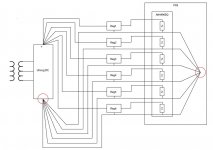
I think the first block diagram below illustrates the problem. A star ground inside the red circle on the left, and another one inside the red circle on the right. I think you're suggesting that I eliminate the star on the right. Unfortunately, that is etched into the PCB, and eliminating it would require a bit of cutting, slicing, and dicing on the PCB. I also think there must be a reason the engineer who designed the evaluation board must have had good reasons to join the grounds like this under the chip. Maybe he had completely independent supplies with no connections to each other, and he decided that this was the best location to join the grounds.
I have a spare PCB, so I could try it.
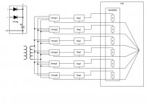
But I wonder if I can solve the problem in the way shown in the second block diagram below. I could use 6 unregulated supplies powered by a single transformer. Do you think this would work?
Dave Halbakken
I think the first block diagram below illustrates the problem. A star ground inside the red circle on the left, and another one inside the red circle on the right. I think you're suggesting that I eliminate the star on the right. Unfortunately, that is etched into the PCB, and eliminating it would require a bit of cutting, slicing, and dicing on the PCB. I also think there must be a reason the engineer who designed the evaluation board must have had good reasons to join the grounds like this under the chip. Maybe he had completely independent supplies with no connections to each other, and he decided that this was the best location to join the grounds.
I have a spare PCB, so I could try it.
But I wonder if I can solve the problem in the way shown in the second block diagram below. I could use 6 unregulated supplies powered by a single transformer. Do you think this would work?
Dave Halbakken
Attachments
Single contiguous Ground plane... would be my first choice or an analogue and digital ground...
If you read the data sheet you get this:
have a look at Henry Ott and others regarding this.
Further, if you look at the data sheet for the EB, you will notice that the grounds all tie together on the motherboard (page 46).
https://www.akm.com/akm/en/file/ev-board-manual/AK4490EQ.pdf
Now if I was doing this layout I would use very small LDO regulators near the supply pins or maybe just use a Pi filter for each supply pin and have one ground (or maybe an analogue and digital plane for initial layout combining them when finished) again as stated in the data sheet.....
If you read the data sheet you get this:
1. Grounding and Power Supply Decoupling
To minimize coupling by digital noise, decoupling capacitors should be connected to AVDD and DVDD
respectively. VREFHL/R and VDDL/R are supplied from analog supply in system, and AVDD and DVDD are
supplied from digital supply in system. Power lines of VREFHL/R and VDDL/R should be distributed
separately from the point with low impedance of regulator etc. AVSS, DVSS, VSSL and VSSR must be
connected to the same analog ground plane. Decoupling capacitors for high frequency should be
placed as near as possible to the supply pin.
2. Voltage Reference
The differential voltage between VREFHL/R and VREFLL/R sets the analog output range. The VREFHL/R pin
is normally connected to AVDD, and the VREFLL/R pin is normally connected to VSS1/2/3. VREFHL/R and
VREFLL/R should be connected with a 0.1µF ceramic capacitor as near as possible to the pin to eliminate the
effects of high frequency noise. No load current may be drawn from VCML/R pin. All signals, especially
clocks, should be kept away from the VREFHL/R and VREFLL/R pins in order to avoid unwanted noise
coupling into the AK4490.
have a look at Henry Ott and others regarding this.
Further, if you look at the data sheet for the EB, you will notice that the grounds all tie together on the motherboard (page 46).
https://www.akm.com/akm/en/file/ev-board-manual/AK4490EQ.pdf
Now if I was doing this layout I would use very small LDO regulators near the supply pins or maybe just use a Pi filter for each supply pin and have one ground (or maybe an analogue and digital plane for initial layout combining them when finished) again as stated in the data sheet.....
Last edited:
Thanks much for your reply, Jan.
I think the first block diagram below illustrates the problem. A star ground inside the red circle on the left, and another one inside the red circle on the right. I think you're suggesting that I eliminate the star on the right. Unfortunately, that is etched into the PCB, and eliminating it would require a bit of cutting, slicing, and dicing on the PCB. I also think there must be a reason the engineer who designed the evaluation board must have had good reasons to join the grounds like this under the chip. Maybe he had completely independent supplies with no connections to each other, and he decided that this was the best location to join the grounds.
I have a spare PCB, so I could try it.
But I wonder if I can solve the problem in the way shown in the second block diagram below. I could use 6 unregulated supplies powered by a single transformer. Do you think this would work?
Dave Halbakken
Yes ideally, you really don't need the star in the right of the diagram.
What you would want to do is place the reg as close as possible to the DAC chip.
The right diagram is not clear to me. All the reg grounds come together but they do not seem to connect to the center tap/cap ground of the raw supply. Unless I miss something.
What I would do is run a single thick wire from the center tap/cap ground to that star.
Then at least all levels are OK and none of the reg local grounds are mixed up with others.
Jan
Last edited:
I concur with Marce, the reason these mixed signal parts tend of have Agnd and Dgnd pins (in multiple permutations) has NOTHING to do with the off chip ground and everything to do with eliminating common impedance coupling due to the impedance of the bond wires and pins....
A nice solid ground pour is best in almost all small signal cases, that whole star ground thing is a strictly low frequency solution, and DACs are in some sense RF parts not audio frequency ones.
A solid plane spaced closely to the top of the board is what my instinct is saying, do it on 4 layers and use a 0.1 - 0.2mm or so spacing between layers 1-2 and 3-4.
4 Layers adds little cost but makes proper grounding so much easier.
Regards, Dan.
I'd do it like this...
Main regulator to take the voltage down to make an easy load for the LDOs, done on loads of designs and is common practice when multiple voltages are required.
Though as said you can have say 1 3V3 and isolate digital and analogue with a PI filter. just doing a complex ADC/DAC board now, not audio but the same problems, making things to complex can increase the noise or create a difference between the various grounds so your resolution can go downhill.
I also concur on the layer stack from DMILLS...
Attachments
Many thanks for all the comments!
Marce - thanks for pointing out that "AVSS, DVSS, VSSL and VSSR must be connected to the same analog ground plane" per the datasheet. That's a pretty convincing argument that the motherboard has a continuous ground plane underneath the daughterboard.
Looking at the layout of the motherboard at 100% in the pdf viewer makes it look as if there is a continuous ground plane underneath the daughterboard. But zooming in with the pdf viewer, it no longer looks so clear-cut. That's one thing I'm confused about. With higher zooming it looks as if a separate ground area might exist for each supply. It is unclear whether this is just an artifact of the pdf output from the pcb layout software, or whether there should actually be gaps between these areas.
Also, thanks for the reference to Henry Ott. I read him a few months ago, but I could not remember his name. Now I can go back and review his notes about grounding and mixed signals.
My intention is to use 4 of these DAC daughterboards in an 8 channel DAC. If I were to use 6 LDOs for each daughterboard, I'd end up with 24 of them. Or fewer if I were to supply left and right channels from the same LDO per your diagram. The least expensive, low-noise, DIY friendly LDO that I've found is the ADM7150, which for so many pieces would be pretty costly. Also I'd like to run the analog stages (VDDR/L and reference voltages) at 6.8 - 7.0 V to squeeze a bit more performance from the chip. I don't see an ADM7150 that produces more than 5V.
Besides, this DAC does not require much current (22 mA typical - 35 mA max on each VDD pin), so I thought the PFM flea regulator might be a likely candidate instead of LDOs. I've breadboarded a flea with an NE5534; it seems to work fine at 30 mA, but I do not yet have a way to measure the noise.
Maybe a super-regulator (Jung or other) supplying higher current, along with pi filters for separation before feeding the pins on the board edge would be better. I don't know, and I'm unsure how to decide.
dmills - I'm sure you're right that a solid ground pour and 4 layers is best. But I don't trust my pcb layout skills to get everything right. That's why I replicated the daughterboard of the evaluation kit. I figured AK must know what they're doing, and perhaps that is the layout they used to do their published measurements.
So, for the moment I'm stuck with 6 copies of that daughterboard manufactured by OSH Park. I'd like to make them work.
You mentioned that the reason for separating pins for analog and digital has "everything to do with eliminating common impedance coupling due to the impedance of the bond wires and pins." Is that also true of separating pins for left versus right channel supplies? I'm not sure how to decide whether supplying left and right channels from separate regulators or just a single regulator is best.
Jan - yes perhaps a big wire to the star ground built into the pcb is the way to go. Or maybe mount the daughterboard above a ground plane and connect that star ground to the ground plane. That doesn't seem very easy mechanically, though. Please ignore my second diagram. It will not solve my problem, which was to avoid multiple ground paths.
I'm still confused why AK engineers created that star (the right-hand star in my diagram) on the daughterboard, and also seem to have connected all the grounds on the daughterboard pcb edges to a single ground plane undeneath. This seems to create multiple ground paths.
Dave Halbakken
Many thanks for all the comments!
Marce - thanks for pointing out that "AVSS, DVSS, VSSL and VSSR must be connected to the same analog ground plane" per the datasheet. That's a pretty convincing argument that the motherboard has a continuous ground plane underneath the daughterboard.
Looking at the layout of the motherboard at 100% in the pdf viewer makes it look as if there is a continuous ground plane underneath the daughterboard. But zooming in with the pdf viewer, it no longer looks so clear-cut. That's one thing I'm confused about. With higher zooming it looks as if a separate ground area might exist for each supply. It is unclear whether this is just an artifact of the pdf output from the pcb layout software, or whether there should actually be gaps between these areas.
Dave Halbakken
That's an artefact of the way the artwork has been produced, unfilled draws, you would not create a real working artwork (Gerber) this way, all routes and pours would be filled. Look at a route it just shows the path as unfilled polygons.
This is a good easy to understand primer... From John Wu & TI.
http://www.x2y.com/filters/TechDay0...log_Designs_Demand_GoodPCBLayouts _JohnWu.pdf
http://www.x2y.com/filters/TechDay0...log_Designs_Demand_GoodPCBLayouts _JohnWu.pdf
Evaluation board... are there to evaluate a product so are a compromise because it has to be flexible, when it comes to a finished product you have all the certification (EMC, FCC) to get through and more intensive testing and signal integrity requirements.
I am doing a multi channel FPGA/ADC/DAC board at the moment, 2000+ components, numerous supplies, bloody horrible M38999 connectors, probably going to go to 10 layers because I want a couple of extra ground layers and all this care to ensure we get a full 14 bit resolution, its all down to very careful layout with converters...
I am doing a multi channel FPGA/ADC/DAC board at the moment, 2000+ components, numerous supplies, bloody horrible M38999 connectors, probably going to go to 10 layers because I want a couple of extra ground layers and all this care to ensure we get a full 14 bit resolution, its all down to very careful layout with converters...
Many thanks for all the comments!
I'm still confused why AK engineers created that star (the right-hand star in my diagram) on the daughterboard, and also seem to have connected all the grounds on the daughterboard pcb edges to a single ground plane undeneath. This seems to create multiple ground paths.
Dave Halbakken
It isn't a star as such, it is slots in the ground plane to control current paths, you have a two layer board so you do NOT have a ground plane, you have ground pours that have numerous slots in them (again Henry Ott and others will tell you how bad this is) so the design is already compromised from a signal integrity and EMC point of view. Looking at the data rates this chip has to handle I would not go less than 4 layers and on a complete product with supplies and any interface IC's would probably look at 6 to 8 with multiple ground layers. It is an evaluation board and not the best example of a low noise high resolution DAC layout. So the slots are to cater for to some extent the lack of a true ground plane...
having looked at the data sheets I have formed a basic picture of how I would lay out this device and its supplies...
I concur with Marce, the reason these mixed signal parts tend of have Agnd and Dgnd pins (in multiple permutations) has NOTHING to do with the off chip ground and everything to do with eliminating common impedance coupling due to the impedance of the bond wires and pins....
A nice solid ground pour is best in almost all small signal cases, that whole star ground thing is a strictly low frequency solution, and DACs are in some sense RF parts not audio frequency ones.
A solid plane spaced closely to the top of the board is what my instinct is saying, do it on 4 layers and use a 0.1 - 0.2mm or so spacing between layers 1-2 and 3-4.
4 Layers adds little cost but makes proper grounding so much easier.
Regards, Dan.
Can't see I disagree, but the OP has an existing PCB with a ground poor under the chip. I believe that in this situation the suggested approach is pretty much as effective.
Jan
marce -
That Wu primer was pretty good. Not that I can do all the math, but his main points make sense. I also learned about a kind of component I'd never heard of before: an X2Y capacitor.
I followed one of his references to this page:
Analog Devices: Analog Dialogue: Ask The Applications Engineer - 12
That page gave a good, simple explanation of why an ADC/DAC analog and digital grounds should be connected to a single, solid ground plane. I'll try a motherboard with a solid ground plane under one of my daughterboards and see what happens.
You wrote, "I am doing a multi channel FPGA/ADC/DAC board at the moment..." Are you doing something like a militarized Red Pitaya board?
You also wrote, "I have formed a basic picture of how I would lay out this device and its supplies..." If you'd be willing to give us a rough idea of your basic picture, it would be much appreciated! I can't be the only one struggling with DAC pcb layout issues. The AK4490 is a pretty good DAC to my ears so far, and one of the reasons I'm in the middle of this issue is because the board I've listened to has a layout that seems poor. Other pcbs for this chip from vendors that frequent diyaudio, though perhaps better, have been subject to criticism, too.
Dave Halbakken
Nope, hi end industrial, the M38999 connectors are fool proof and don't come apart, plus they are sealed, used in planes trains and automobiles as well. 7000+ pins 🙂
I like the John Wu link its clear and concise.
I like the John Wu link its clear and concise.
Sorry, no, I haven't had a chance to listen to it. Is it good?
Did you try the Mirand dac?
Ciao, george
- Status
- Not open for further replies.
- Home
- Source & Line
- Digital Line Level
- Connecting multiple voltage regs to DAC board?