The literature usually just states that emitter followers have a voltage gain of 1 -- but I would like to know how to compute that with a bit better accuracy.
With a 1 kHz sine wave, on point A I measure 4.36 Vp-p, and 4.04 Vp-p on point B, so the voltage gain is 0,9266.
The current through the driver (Q1) is 920uA, and the DC bias is right on target at +5VDC.
I tried to simulate the whole circuit in Multisim, and it's giving me identical Vp-p values for A and B, and that is most certainly not correct.
Try a much lower load value, like 1k or even 100R. It's essentially open circuit with 100k.
Last edited:

Did your test use 100R or 100k? It should show some source impedance with 100R loading,
although C1 will have to be larger now.
although C1 will have to be larger now.
The gain of 1 rule of thumb is small signal. Much more complicated for large signal. Did you use transient analysis or AC in the sim?
The gain of 1 -- as far as I can tell -- is just a rough, 1st approximation. There has to be a more precise way to describe the actual voltage gain, which should be more or less independent of signal level -- provided, there is no clipping or cross-over distortion. I'm fairly certain there is some equation that correctly describes that, but I was unable to find it.
BTW, I made some minor changes to the Multisim circuit, and now it's correctly simulating the voltages -- 4.40 Vp-p @A and 4.00 Vp-p @B.
BTW, I made some minor changes to the Multisim circuit, and now it's correctly simulating the voltages -- 4.40 Vp-p @A and 4.00 Vp-p @B.
Last edited:
Replace both transistors with voltage-controlled current sources with a transconductance gm = IC/(kT/q), where k is Boltzmann's constant, T the absolute temperature and q the absolute value of the electron charge. kT/q is about 25.69 mV at 25 degrees Celsius.
Add a resistance of hfe times 1/gm between what used to be the base and emitter. See if you can find a datasheet showing the slope of the collector current with collector-emitter voltage and use that to find out what internal resistance to put between the collector and emitter terminals - or just neglect it, as it's probably the 100 ohm that dominates anyway.
Replace the diodes with resistors with a value n(kT/q)/IF, where n is the emission coefficient, about 1.9 for 1N4148. Replace the capacitors with short circuits.
Now look up modified nodal analysis and solve the network equations.
Last edited:
If the effect of the diodes is negligible, you can also just sum the transconductances, calculate the parallel value of the 100 ohm load resistor and the two internal resistances and calculate gm,totrL/(gm,totrL + 1), where gm,tot is the total transconductance and rL the parallel value of the 100 ohm and internal resistances. It's at least closer to the correct value than 1.
A practical circuit will need emitter resistors on Q1 and Q2. It will also need some means to adjust the bias current - or make the voltage drop across the emitter resistors large enough to swamp differences in voltages across the diodes and base-emitter junctions.
Once the current in Q1 and Q2 is known, the small-signal resistance looking into an emitter is 1/gm.
Ed
Once the current in Q1 and Q2 is known, the small-signal resistance looking into an emitter is 1/gm.
Ed
1. Assume the NPN and PNP devices are perfectly complements. Same |Vbe| , same |hFE| , same hybrid-pi model parameters. Be sure to include hybrid-pi parameter "ro" which models the Early effect in bipolar transistors. It's why real transistors have IV curves that slope upwards, unlike ideal transistors whose IV curves are flat and perfectly horizontal.
2. Follow the excellent advice in posts 7 and 8 above.
_
2. Follow the excellent advice in posts 7 and 8 above.
_
Attachments
Transistor circuit like this have voltage gain less than one , because it's a current amplifier , which have voltage drop base-emitter anyway , and dc current gain is load current dependent. In real circuit , as was mentioned in post #10 , transistor current curves are no flat. So only with infinte load you may have something close to same gain for all amplitufes .Real transistor may have gain 500 at 1ma collector current, at 10ma maybe 400 ,at 50ma maybe 300 , and so on. Even if your signal source have zero ohms output resistance and don't sag with load , transistor will amplify current less with harder load (less ohms) , and output voltage will decrease. Probably there begins distortions.
Only very complicated models in simulations can be partially close to real transistor behaving in circuit.
Only very complicated models in simulations can be partially close to real transistor behaving in circuit.
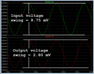
Here's what I got in a .TRANsient analysis using relatively small signal amplitudes (less than 10 millivolts). I think you'd also find .AC analysis to be useful.
Gain from node A to node B was way, way less than +1. It was +0.32 volts per volt. LTSPICE results attached below.
I used the ".MEASURE" feature of LTSPICE to have the simulator extract the peak-to-peak ("PP" in the measure command) amplitude at node A and also at node B, from 2 msec to 5 msec. Those amplitudes are shown in attachment 1.
_
Attachments


A practical circuit will need emitter resistors on Q1 and Q2. It will also need some means to adjust the bias current - or make the voltage drop across the emitter resistors large enough to swamp differences in voltages across the diodes and base-emitter junctions.
Good point, I completely overlooked that at 6 AM. An alternative is using dual matched transistors and replacing D1 and D2 with diode-connected transistors.
I think there are (crazy) ways to make the circuit work both in real life and in simulation. If you used a tiny dab of cyanoacrylate superglue to bond D1 to Q1, and also bond D2 to Q2, and also immerse the entire circuit in a bath of Fluorinert liquid coolant (like they used in the Cray-2 supercomputer) circulating at relatively high speeds and cooled to +5C ... then I think the circuit would work. It's not impossible, it's just impractical. Highly impractical.
In addition to temperature variation, Is is not well-matched between D1, D2, Q1, and Q2. The currents in Q1 and Q2 will vary with Is.
Ed
Ed
The original circuit, including the VAS works just fine on a breadboard. No visible crossover distortion on the scope, and there's quite a bit of headroom until visible clipping.Thanks. The original circuit is yet another that works only in simulation.
Ed
I'm simply trying to analyze a circuit -- done that with the other portions of the complete circuit, and the numbers I computed agreed very nicely with my measurements. However, I was unable to compute the voltage gain of this stage since there are no emitter resistors and re' didn't give me the right answer when using the Av = Rl/re' + Rl -- I got something around 0,97 for Av, which is way off.
Last edited:
I added parenthesis.aurgathor said:when using the Av = Rl/(re' + Rl) -- I got something around 0,97 for Av, which is way off.
The current in Q1 and Q2 is likely way off the simulated value. You need to use emitter resistors and a better bias network to get predictable performance.
ETA: I re-read your original post. I compute Av = 100/(100+.02585/920e-6/2) = 0.87. The signal amplitude is large enough to make the small-signal analysis break down.
Ed
Last edited:
Yes, the 20.2 mA peak output current is a lot more than the 920 uA quiescent current.
When you simplify the situation by assuming that the current through the diodes is constant, that there are no thermal issues and that Early effect can be neglected, you can calculate what input voltage excursion is needed for a given output voltage excursion, using the fact that the output stage is a product rule class-(A)B stage:

When you simplify the situation by assuming that the current through the diodes is constant, that there are no thermal issues and that Early effect can be neglected, you can calculate what input voltage excursion is needed for a given output voltage excursion, using the fact that the output stage is a product rule class-(A)B stage:
- Home
- Amplifiers
- Solid State
- Computing voltage gain of complementary emitter follower