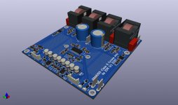
Lockdown in Belgium is starting to give results - here's my latest design with TPA3255🙂
Boards:
https://sites.google.com/view/dacgear/
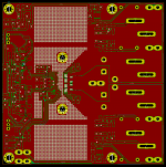
- Compact low cost 10x10cm PCB with wide output tracks
- PFFB built in
- Stereo BTL configuration only
- Differential or SE inputs
- Minimized capacitors in signal path, opamps running on +-4.75V with voltage inverter
- Single 53V power supply, 12V and 5V derived with LM5017 step down converter.
- Coilcraft or generic toroid coils can both be used on board.
Boards:
https://sites.google.com/view/dacgear/
Attachments
Last edited:
LT3012 seems to be a linear voltage regulator. And is about 5eu(!) a piece, plus taxes.
Yes, you are right. Previous one I used was buck converter, so it just slipped in. I didn't even check the price to be honest, I got it as a sample. Anyway, there is a connector for external 12V PS, if someone needs it.
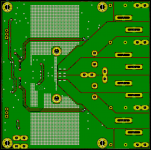
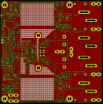
This GND plane is Not good für Audio...
IT IS like the cheap China amplifiers...
You have used lots of vias.
But most of them on the wrong Place.
You have to priorize correct Signals...
IT IS like the cheap China amplifiers...
You have used lots of vias.
But most of them on the wrong Place.
You have to priorize correct Signals...
Last edited:
I don’t understand what you mean. If you see a specific issue, please use electrical engineering terminology to describe it, I am an electronic engineer after all.
I don’t understand what you mean. If you see a specific issue, please use electrical engineering terminology to describe it, I am an electronic engineer after all.
You no see troubles? Show me current path from caps to GND pins TPA3255
See described current path from capacitor to Chip.
The +48V Input ist OK.
But the GND Input hast to be also short as possible and routed directly to the Chip GND
Your GND plane on top layer is connected to the Caps, OK.
But then there are only a few vias near the outline to Connect to the bottom layer.
And after then it is connected to the Chip.
Additional , These GND plane is cutted from the PFFB Feedback signals.
This Part ist also the more critical Part of Signal.
So i would move the PFFB components to Input parts AS Close ad possible
In additional See GND path from capacitor to other GND of Signal Input.
To make it more easy to See, use a pencil (, different colours) and Paint the current path in your Layout.
One time for Power amplifier, one for additional Power (12V)
And a third one for the Input GND.
In additional ... I think your LDO will be very hot.
I dont know the consumption of tpa @12v..
But a voltage drop of about 36V is to much ..
for calculation: Iout x Vdrop -> 3,6W of thermal Power
If the Chip use 100mA @12v
Last edited:
That is why I choosed a flybuck regulator in my design delivering +/-12V.In additional ... I think your LDO will be very hot.
I dont know the consumption of tpa @12v..
But a voltage drop of about 36V is to much ..
for calculation: Iout x Vdrop -> 3,6W of thermal Power
If the Chip use 100mA @12v
The quality of the pcb-layout will be measurable by carrying out a simple THD-measurement at 1kHz. You will notice much more k2 than TI shows for their reference design. It took me several iterations to be on par with this one.

You no see troubles? Show me current path from caps to GND pins TPA3255
I hate to admit it, but you are right! I will have to put a thick jumper on top of the top layer, don't see another way.
No you have to do better routing on the top, or maybe use jumpers there. Groundplane should not be broken up.
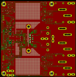

I think the LDO is self-desoldering ^^
Ist would be better to use an external Power supply 15V ... Or use of an 15v amps and then the LDO's
Ist would be better to use an external Power supply 15V ... Or use of an 15v amps and then the LDO's
- Home
- Amplifiers
- Class D
- Compact TPA3255 design with PFFB and single PS