Some changes were required to improve the thermal behavior of the amplifier. Moving transistors Q15 and Q16 to the heatsink to sense temperature of the output transistors proved to produce overcompensation with bias current on output transistors being pushed down to 0mA. Much improved behavior was obtained by thermally coupling pairs Q15/Q18 and Q16/Q17, both isolated from the heatsink. Bias current was measured to remain constant after several tests including sine wave at 60% max power and music reproduction driving speakers. That suggests that sensing the current on the ballast resistors is a valid (better?) alternative to sensing the usual Vgs+R voltage.
One unexpected behavior of leaving the power source followers out of the overall feedback loop: the crossover distortion gets reduced significantly. The bias current needs to be increased up to fivefold to notice distortion on the scope. I cannot find the reason for this, otherwise a positive result.
Perhaps due to the feedback of gate capacitance current via Q15/Q16 and the lack of compensation in the first two stages (high bandwidth), the crossover distortion is being corrected by global feedback?One unexpected behavior of leaving the power source followers out of the overall feedback loop: the crossover distortion gets reduced significantly. The bias current needs to be increased up to fivefold to notice distortion on the scope. I cannot find the reason for this, otherwise a positive result.
Late to the party, maybe it has already be mentioned, but is the input impedance of such a circuit very low?
Jan
Jan
Some changes were required to improve the thermal behavior of the amplifier. Moving transistors Q15 and Q16 to the heatsink to sense temperature of the output transistors proved to produce overcompensation with bias current on output transistors being pushed down to 0mA. Much improved behavior was obtained by thermally coupling pairs Q15/Q18 and Q16/Q17, both isolated from the heatsink. Bias current was measured to remain constant after several tests including sine wave at 60% max power and music reproduction driving speakers.
For the necessary thermal stabilization of the circuit, you need to increase the current through the Q13Q14 driver transistors to 14mA. This can be done by increasing the resistance R9R10 from 56 ohms to 82 ohms.
By selecting the value of R40, you can set the zero point at the output of the circuit.
Attachments
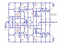
there is no global feedback. The power source followers that connect to the speaker output operate open loop.Perhaps due to the feedback of gate capacitance current via Q15/Q16 and the lack of compensation in the first two stages (high bandwidth), the crossover distortion is being corrected by global feedback?
Please note that the collector current in Q13 has to be half the collector current of Q11. This way collector curren of Q11 split half to Q16, half to Q17. Actually current in Q17 a little higher to provide adequate bias to the output MOS. The same for the other.half of the complementary stage.For the necessary thermal stabilization of the circuit, you need to increase the current through the Q13Q14 driver transistors to 14mA. This can be done by increasing the resistance R9R10 from 56 ohms to 82 ohms.
By selecting the value of R40, you can set the zero point at the output of the circuit.
It is 10kohms. It could be considered low by some. But most preamplifiers have output impedance in the 100's. It is easy to rise that value to say 20k/50k but I like to have (relatively) low impedance connections (better connector contact?). Cannot justify really!Late to the party, maybe it has already be mentioned, but is the input impedance of such a circuit very low?
Jan
Actually to have a flat input impedance there is a need to include a small cap in parallel to the feedback resistor R37. It also extends the bandwidth to a few hundred kHz. Not verified with my very basic test setup (REW, 20kHz).It is 10kohms. It could be considered low by some. But most preamplifiers have output impedance in the 100's. It is easy to rise that value to say 20k/50k but I like to have (relatively) low impedance connections (better connector contact?). Cannot justify really!
No much dependence on bias current, the input impedance of the common base transistors is in the order of a few tens of ohms. The local feedback loop (R5/R7=10) rises that impedance to near 25k (250k collector resistance over local R5/R7, referring here to only half the complementary circuit).So that input impedance depends on the bias current in the input stage, right?
Jan
But input impedance depends more strongly on the overall feedback given by R37, current feedback into the input node . The higher the frequency the lower the forward gain and that has an impact on the input impedance (raises with frequency). A capacitor in parallel with R37 increases feedback at higher frequencies and the result is better control of the input impedance. The capacitor is not shown in the schematic.
she there is.there is no global feedback.
the circuit is closed through Q15Q16 and Q17Q18, i.e. the overall feedback is non-linear.The power source followers that connect to the speaker output operate open loop.
Last edited:
the minimum ratio is the square root of 2, and this condition is met, when the current through KQ13 is 14mA, through Q11 the current is 25mAPlease note that the collector current in Q13 has to be half the collector current of Q11.
like this?Actually to have a flat input impedance there is a need to include a small cap in parallel to the feedback resistor R37.
As the transistor arrangement in @tucura's circuit from post 1 is inexplicably interesting to me, I ran some comparative sims of the full circuit (based on the file posted by @IanHegglun in post 37), the complementary 2T input stage, and complementary 1T IPS (Q6 and Q22 from original post removed, AC impedances and DC bias points set approximately equal).Late to the party, maybe it has already be mentioned, but is the input impedance of such a circuit very low?
Jan
Input impedances at 1kHz were as follows with 10K input RG:
Full circuit, GNFB connected: 9.99k
Full circuit, GNFB disconnected: 7.39k
2T Complementary IPS: 6.65k
1T Complementary IPS: 6.73k
With 1G RG:
Full, with GNFB: 198.22k
Full, no GNFB: 22.93k
2T: 16.67k
1T: 17.27k
With 1G RG, input impedance rises 3dB at 6-7hz and falls 3dB around 29kHz for the 1T and 2T circuits, around 44kHz for the full circuit without feedback. For the circuit with feedback and 1G RG, it's +1dB at 1hz and -3dB at 10kHz. With 10K RG and feedback connected as in the original post, input impedance is only +.5dB at 1hz and and is -3db at 192kHz.
Attachments
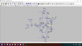
I'm very sorry, I cannot follow your elaboration. I want only to mention that R18 (it fixes the input impedance) is 10kohms (not 1Gohm).
Sorry if my post wasn't clear. I compared the original circuit, the common base input stage on its own, and a complementary common emitter stage with bias point and surrounding impedances matched to those in the common base stage. I simulated the full circuit twice, once with the global feedback connected and once with it disconnected.
I ran AC simulations to get small signal input impedance. First, I ran simulations on each circuit with R18 at 10K, which is where I got the first set of numbers. Then I changed R18 to 1G to essentially eliminate it and more clearly expose the inherent input impedance of the circuit, which gave the second set of numbers. For flexibility in simulating multiple situations, it was easier to change R18 to 1G than to simply delete it.
The main point of interest for me is seeing that the common base/common emitter (Blesser Super Transistor) arrangement has a very similar input impedance to a common emitter alone.
One correction to the original numbers: The slight impedance discrepancy between the common base input stage alone and the full circuit without feedback was due to Ian and I using different models for the MJE340. When using identical models, the input impedance for the two circuits become essentially identical.
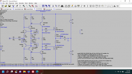
As I mentioned in a previous post #62 there is an unexplained (by me!) result of leaving the source followers out of the overall feedback loop as described in post #43. Attached are simulation results of forcing 1Amp/10kHz sine current into the speaker output of the amplifier, with overall feedback in one case, and leaving source followers out of the loop in the second case. The difference in terms of crossover distortion is very significant. As shown in the plots, goes from barely noticeable to be as large as the signal itself. Very high signal current forced into the amplifier is not uncommon whenever speaker impedance is inductive, usually at very low frequencies. It is also clear from the plot that overall feedback also increases damping significantly. I have to setup the circuit in a way than I can try both cases with music to determine what sounds best: high damping or low crossover distortion!
Attachments
R37 does not have to be connected to the bases re Q17 Q1818, you can add a 0.15 uF capacitor in series R37 so that the time constant corresponds to R50C5, and reconnect this circuit immediately to the amplifier output - this will increase the linearity of the amplifier and stabilize the operating point.
In a model with such refinement, it turns out very well.
In a model with such refinement, it turns out very well.
- Home
- Amplifiers
- Solid State
- Common-base input for power amplifier