Back in 1995 I designed a 250W/channel power amplifier. A few thousands were fabricated before the company went into financial troubles and ended production shortly thereafter. The circuit met my design target of achieving required performance with a minimum number of circuit nodes, and that motivated a refuse to adopt the traditional circuit architecture (differential pair, voltage amplifier and follower) that I consider useful only for operational amplifiers. There are a number of comments in this forum suggesting that the voltage amplifier requires an additional buffer stage to drive the power MOS. This stage would eventually handle the high input capacitance of the output devices. The shown design uses high enough current on the voltage gain stage and that sufficed, at least did in this particular case, to provide adequate drive to 6 power MOS gates. The input stage, unusual for power amplifiers, uses a complementary common-base connection, that provides high enough input impedance due to voltage feedback from the following stage. The motivation to design a circuit with a minimum number of nodes is to reduce the number of parasitic poles. The technique proven correct, since it made possible to provide adequate stability margin without the use of an additional Miller capacitor for frequency compensation.


The Hitachis. Nice, but obsolete for decades now.These are lateral fets, right?
this is not a problem,there are substitutes and they are also very easily found in second-hand amps.The Hitachis. Nice, but obsolete for decades now.
yes, Hitachi lateral mosfets. As far as I remember other power MOS were later tried but performance with Hitachi's was best (crossover distortion). Not sure why.
Have you tried with single output pair at let's say +/-35V ?yes, Hitachi lateral mosfets. As far as I remember other power MOS were later tried but performance with Hitachi's was best (crossover distortion). Not sure why.
You can buy a current range of lateral power mosfets, including equivalents to obsolete Renesas/Hitachi TO3P types here - https://www.profusionplc.com/type/lateral-mosfet. So you can still build whatever lateral mosfet design you like with genuine new components.
I see they have now put TO3 laterals on "end of life", but you can still get TO247 versions OK.You can buy a current range of lateral power mosfets, including equivalents to obsolete Renesas/Hitachi TO3P types here - https://www.profusionplc.com/type/lateral-mosfet. So you can still build whatever lateral mosfet design you like with genuine new components.
the first few tests were done using a single pair and half the supply voltage. But performance was not measured. Only proper operation was verified. That was back in 1995 then my memories are nothing to be trusted.Have you tried with single output pair at let's say +/-35V ?
It would be "high" given that there are 3 voltage gain stages (common-base, common-source & common-source) but the first 2 have very high local feedback, then is difficult to say. At that time my only concern regarding feedback was to prevent overload during input voltage steps. The feedback loop encompasses all 4 stages and that causes high currents spikes (voltages difficult to see) in almost all devices, something I consider a potencial source of "problems". I am now working on a new design (after 25 years) to take care of this issue.I like the input stage much.
By what letter could we replace x in this x Feedback Amplifier ?
It would be "high" given that there are 3 voltage gain stages (common-base, common-source & common-source) but the first 2 have very high local feedback, then is difficult to say. At that time my only concern regarding feedback was to prevent overload during input voltage steps. The feedback loop encompasses all 4 stages and that causes high currents spikes (voltages difficult to see) in almost all devices, something I consider a potencial source of "problems". I am now working on a new design (after 25 years) to take care of this issue.
Are you talking about high current spikes in the output devices only, or somewhere else?
Did you measure the THD of this design? I'd be interested to know how it performed.
That configuration of input transistors turns the left emitter into the composite base. So this circuit ends up as a CFA with the input at the high impedance input and the feedback at the low impedance input. At least that's how it looks to me. https://www.diyaudio.com/community/threads/bob-cordells-power-amplifier-book.171159/post-4909328
Hola colega 😉 con qué marca los vendían?Back in 1995 I designed a 250W/channel power amplifier. A few thousands were fabricated ...
Hi partner, interesting, what brand were they sold under?
Never heard of commercial Lateral Mosfet use before (in Argentina that is) because they were always very expensive and hard to get here.
As a side note, the 90´s were HARD for any local manufacturer, 1:1 de facto dollarization plus never stopped inflation meant imported stuff was sold way below our local manufacturing cost .... unfair competition and impossible to sustain.
Many/most excellent product manufacturers bit the dust and had to close.
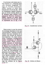
The paper in french was published in L'Audiophile n°40, first quarter of 1987. An author quoted by Self, Staric and Margan for the circuit of the differential input pair plus emitter follower is Schlotzaur.That input configuration was described in 1970 paper (attached reference is in french):
Here is Blesser's letter in English:That input configuration was described in 1970 paper (attached reference is in french):


An alternative emitter driven Blesser arrangement to Post 1 was posted by dadod (Damir) here https://www.diyaudio.com/community/threads/bob-cordells-power-amplifier-book.171159/post-4909712
Dado's circuit appears to me to be a better arrangement than the standard voltage-driven output stage because there are negligible high-order harmonics, just low order harmonics which reduces the need for so much negative feedback in an amplifier.
To discover its inner workings I first simulated dadod's circuit as Common Emitter, not as a follower but in open-loop (see below)


I used dadod's circuit with BC550/560 output transistors but with a 300 ohm load. To get 15V output swing requires 50mA peak which is just within the transistors ratings. It's close enough to check out feasibility for an output stage. Here the idle current is about 2mA.
In open-loop gain is not very linear, the Gm at idle rises by a factor of 4 at the peaks because each output transistors gain is close to a cube-law. But with negative feedback (such as a follower) the distortion is acceptable.
So it looks like the bias current is too low? Well, strangely, increasing the idle current does not give the familiar "optimum bias" for low distortion like standard voltage-driven (optimally biased Class-AB) output stages. Here the bias is set to 2mA for 50mA peak to compare with standard voltage-driven optimally biased Class-AB output stages - which typically have an idle current in the range of 1/20th to 1/50th of the peak output current,
So with this Blesser emitter driven circuit we have this cube-law like nonlinear gain which is very different to standard voltage-driven optimally biased Class-AB output stages. But I consider to be a good thing for audio amplifiers, or at least better harmonic profile than from standard voltage-driven output stages (see my next post for distortion for the follower).
Another advantage of this Blesser arrangement is emitter resistors are not needed for the output transistors. This is because the output transistors are current amplifiers, ie, they are current driven. To parallel output transistors you use 'slicing' by paralleling several Blesser stages (similar to the LT1166 and my autobias circuits eg here).
Notice the bases of the output transistors are not linked by the usual Vbe multiplier to set the idle bias current, instead the bases are driven by a very high impedance, hence they are current driven and the pull-up current sources (I2,I4) needs to be sufficient to give the peak output current which is Beta times this current source current. This results in a wider and smoother crossover where one output transistor remains slightly active over the full output range, ie it is "non-switching".
So this Blesser emitter driven circuit is similar to autobias and sliding bias arrangements where the bases of the output transistors are not linked by the usual Vbe multiplier to set the idle bias current, The idle current is set by the sum of R7 and R8 which need to be an NTC with a temp.co of about 2%/C to prevent thermal runaway of the output transistors. It is also important to limit the input drive to the emitters to prevent loss of bias control where both devices start to conduct above 0.6V input which can destroy the output transistors. Schottky diodes can prevent this.
My next post covers distortion as a follower and its sonic advantage over standard voltage-driven and optimally biased Class-AB output stages
Dado's circuit appears to me to be a better arrangement than the standard voltage-driven output stage because there are negligible high-order harmonics, just low order harmonics which reduces the need for so much negative feedback in an amplifier.
To discover its inner workings I first simulated dadod's circuit as Common Emitter, not as a follower but in open-loop (see below)
I used dadod's circuit with BC550/560 output transistors but with a 300 ohm load. To get 15V output swing requires 50mA peak which is just within the transistors ratings. It's close enough to check out feasibility for an output stage. Here the idle current is about 2mA.
In open-loop gain is not very linear, the Gm at idle rises by a factor of 4 at the peaks because each output transistors gain is close to a cube-law. But with negative feedback (such as a follower) the distortion is acceptable.
So it looks like the bias current is too low? Well, strangely, increasing the idle current does not give the familiar "optimum bias" for low distortion like standard voltage-driven (optimally biased Class-AB) output stages. Here the bias is set to 2mA for 50mA peak to compare with standard voltage-driven optimally biased Class-AB output stages - which typically have an idle current in the range of 1/20th to 1/50th of the peak output current,
So with this Blesser emitter driven circuit we have this cube-law like nonlinear gain which is very different to standard voltage-driven optimally biased Class-AB output stages. But I consider to be a good thing for audio amplifiers, or at least better harmonic profile than from standard voltage-driven output stages (see my next post for distortion for the follower).
Another advantage of this Blesser arrangement is emitter resistors are not needed for the output transistors. This is because the output transistors are current amplifiers, ie, they are current driven. To parallel output transistors you use 'slicing' by paralleling several Blesser stages (similar to the LT1166 and my autobias circuits eg here).
Notice the bases of the output transistors are not linked by the usual Vbe multiplier to set the idle bias current, instead the bases are driven by a very high impedance, hence they are current driven and the pull-up current sources (I2,I4) needs to be sufficient to give the peak output current which is Beta times this current source current. This results in a wider and smoother crossover where one output transistor remains slightly active over the full output range, ie it is "non-switching".
So this Blesser emitter driven circuit is similar to autobias and sliding bias arrangements where the bases of the output transistors are not linked by the usual Vbe multiplier to set the idle bias current, The idle current is set by the sum of R7 and R8 which need to be an NTC with a temp.co of about 2%/C to prevent thermal runaway of the output transistors. It is also important to limit the input drive to the emitters to prevent loss of bias control where both devices start to conduct above 0.6V input which can destroy the output transistors. Schottky diodes can prevent this.
My next post covers distortion as a follower and its sonic advantage over standard voltage-driven and optimally biased Class-AB output stages
Attachments
Now dadod's Blesser output stage as a voltage follower:


The same idle current is used as in the previous post but now there is a lot of local negative voltage feedback to make it quite linear.
The THD at 1V peak output is 0.026% and at 14V 0.07%.
What I find more significant is a the lower output level the harmonics above the 3rd virtually disappear since they fall by about 20dB as you go to the next harmonic. So effectively the only harmonic you would hear at this low output level is the 3rd and we know the third becomes inaudible below about 0.3%. and this circuit is ten times lower than that. Also at the higher level the harmonics still fall fast enough so as the harmonic number is increases we don't get to hear any of the higher harmonics. The rate of fall-off at the higher level is about 60dB/decades and out hearing increases perception as the harmonic number is increases, at about 50dB/decade.
So even at full output swing this circuits distortion remains inaudible. Whereas the standard voltage-driven optimally biased Class-AB output stage has a typical harmonic profile that falls at a rate of -40dB/decade which means we may hear the higher harmonics even when the THD value is very small, even at 0.01% THD crossover distortion of the standard output stage it has been found to be audible.
The upshot is this Blesser/dadod circuit appears to out-perform the standard voltage driven output stage and allows less negative feedback to get distortion inaudible.
The above distortion plots suggest the Blesser/dadod follower output stage has low enough distortion that it does not need any additional global feedback.
Attachments
- Home
- Amplifiers
- Solid State
- Common-base input for power amplifier