Actually R7/R8 are not only degeneration resistors that as such are required to provide some pole splitting when closing the feedback loop, but also provide bias to all the circuits. In effect voltage drop across R7+R8 equals 2*Vbe and that defines bias current to all the circuitry.Hi tucura,
Re Post 31 and R7,R8. That refers to the dadod circuit which is now known to be not a Blesser arrangement. What we need to look at are the same resistors in the "holi-org" circuit of Post 1 circuit - coincidentally the same resistor numbers for the circuit above (Post 37).
R7,R8 "holi-org" circuit act like emitter degeneration resistors in the input stage of a CFA. The mid node of R7,R8 is the equivalent of the inverting input of a CFA. In the circuit above the mid node of R7,R8 I added R18 to common to monitor the current to common. This resistor corresponds to the resistor for a CFA feedback network but it is not used this way for this amp. Instead, the feedback is applied to the emitter resistors equally with two feedback resistors of twice value to one Rf to R18. This trick gives the same feedback effect as a CFA but with a little more feedback depth than the usual CFA method.
It is not derived from the 741 but my first approach was to use an input differential pair similar to the 741 in order to eliminate the double differential pair to have a symmetric configuration. The 741, as shown in the figures I included, allows for using both output of the input pnp/npn compound to generate useful output voltages (don't remember which design of operational amplifier derived from the 741 was using this configuration). Briefly the figures showAre you sure it was the 741? I'm struggling to see any similarity there. Looks like a fairly standard differential input stage.
a) a typical 741 (don't remember exacly if it is the original o an early derivation).
b) a derivation with a different bias.
c) same as b) where both branches are used to generate useful output currents
d) Same circuit with many element eliminated to make the circuit single-ended
e) some elements removed and current sources replaced with resistors.
f) final configuration including transistors that provide adequate bias to the input transistors
I mentioned the original circuit was modified to make it single-ended. I was under the assumption that a differential front end circuit is only mandatory for DC amplifiers. Audio amplifiers are not. The same with current-sources/resistors issue. Finally the pnp/npn 741 style compound was abandoned there is no need to have very high input impedance. The pnp/npn compound (Blesser?) resulted from the need to bias the common base input transistor. The low distortion of this configuration results from the fact that it has a very high open loop gain. The closed loop gain is equal to the input transistor and its collector resistor.
I designed this circuit more than 25 years ago, then not sure all I describe is correct!
Attachments

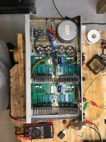
I have finally completed the design of a new version of the power amplifier using a common base front-end circuitry. A prototype built using chassis and power supply from an old, sold for parts, amplifier, I managed to confirm correct operation and compare performance with my old but revered Sony SR-P50 amplifier. The motivation for the new design is to reduce the impact of crossover distortion in the input stage currents, and also to make use of low cost and easy available MOS power devices. The common base configuration is used in both the voltage gain stage and the output follower.
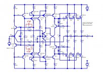
The input stage uses a common base transistor (Q1/Q2) and a pair of voltage followers (Q3,Q5/Q4,Q6) with voltage feedback required to have a closed loop gain of x10. The motivation of using a double follower is to raise the collector voltage operating point of the input transistor. The follower is mirrored with an identical biased device (Q9/Q10) using a technique introduced by Barry Gilbert in some of his many designs since 1960’s. The technique helps to isolate the feedback loop from the output load (improved stability). The mirrored stage (Q9/Q10) combined with common-base transistor (Q11/Q12) to form a folded cascode stage that provides the remainder of the required voltage gain. A resistor (R37) senses the voltage of the output collectors and steers current feedback into the input stage. Current feedback helps to eliminate common mode voltage at the input node. The gain stage of the original design was changed to allow the use of this feedback flavor.
The voltage follower stage (only local feedback) includes a common-base/common-drain circuitry (Q15/Q16 and M1/M2), in this case with 100% voltage feedback to provide unity gain. Current spikes into the collector current of the common-base devices (Q15/Q16) is anyway a significant fraction of the ~8mA collector bias current (not good!). The stage also defines quiescent current of all MOS power transistors. Gate-source voltage is adjusted by sensing bias current directly on the ballast source resistors (R29/R30), configuring a temperature independent bias control loop. Two additional source followers using identical gate voltage (again the mirror concept) provides the output current to the speaker.
The final test result: sound quality much improved, mostly in orchestral tutti, the real weak point of the SR-P50. Please note: no blind tests done, and I suffer severe tinnitus.
This is still in the prototype stage, all comments and suggestions are welcomed. The final implementation requires a new transformer to increase output power to the >100W target, and new PCB if justified by circuit changes. An appropriate chassis will be needed, and that represents a real challenge to my abilities, again suggestions are welcomed.
Attachments
Hello!This is still in the prototype stage, all comments and suggestions are welcomed.
modeled the circuit.
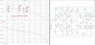
due to the use of local feedback at the input Q13 Q14 Q15 Q16 very high frequency spectrum, it is necessary to limit the spectrum of the input voltage amplifier, because. above 20 MHz, the phase turns in the opposite direction, for this it is necessary to shunt the resistors R7 R8 with a 4.7pF capacitor, see attachment.
The non-linearity of the R37R50 non-feedback amplifier is +/-8dB (1kHz-20kHz). This non-linearity is the result of the Q13Q14's low current driving the high total input capacitance of the 3 pairs of output mosfets. Because Q13Q14 works as part of the Widlar current mirror, simply increasing the current will not work. as an option to add a booster follower before the output mosfets
Attachments
Last edited:
HI Hennady, early on the design tried a similar value capacitor as you suggest (for a different reason though) and could not observe any improvement on final performance. Not sure if you are relating to stability or other performance issues and not sure what do you mean by phase turning into the opposite direction. Regarding stability (one of the problems of having current-current feedback (R37-R50) is that when the input is left open the loop gain increases and stability can suffer. That is the reason to include a first stage (common-base/common-collector with local feedback) having very high bandwidth. Frequency response is then dominated by the second cascode stage. I verified that the circuit is free from oscillation when disconnecting the input from the signal source, something that was of some concern at the beginning of the design.Hello!
modeled the circuit.
due to the use of local feedback at the input Q13 Q14 Q15 Q16 very high frequency spectrum, it is necessary to limit the spectrum of the input voltage amplifier, because. above 20 MHz, the phase turns in the opposite direction, for this it is necessary to shunt the resistors R7 R8 with a 4.7pF capacitor, see attachment.
The non-linearity of the R37R50 non-feedback amplifier is +/-8dB (1kHz-20kHz). This non-linearity is the result of the Q13Q14's low current driving the high total input capacitance of the 3 pairs of output mosfets. Because Q13Q14 works as part of the Widlar current mirror, simply increasing the current will not work. as an option to add a booster follower before the output mosfets
Regarding non-linearity (what do you mean by +/-8dB ?) you relate to the VAS stage (enclosed by R50) but then point as responsible the low current on Q13, which is in the voltage follower stage (only local feedback). I would appreciate if you can elaborate on this issue.
there are 2 reasons:HI Hennady, early on the design tried a similar value capacitor as you suggest (for a different reason though) and could not observe any improvement on final performance.
1st is a relatively highohms feedback divider at the bases of the input transistors.
2nd , the voltage driver gain is in a wider frequency range compared to the second driver before the FETs.
better to seeRegarding non-linearity (what do you mean by +/-8dB ?)
Attachments
look carefully:could not observe any improvement on final performance.
Attachments
Thank you for your efforts in evaluating the circuit. I understand now, you were referring to linear distortion. I will run the ac simulation again and let you know. The final bandwidth reaches 20kHz within a few cents of a dB. My primitive test setup doesn't go beyond 20kHz.better to see
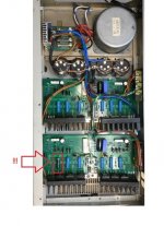
The burnout resistor was the result of a brief short circuit (speaker-ground).
It doesn't matter, because the output stage works in class AB. I have shown the effect of output stage input capacitance on gain linearity without local negative feedback.I will run the ac simulation again and let you know. The final bandwidth reaches 20kHz within a few cents of a dB.
strange that the fuses held. and the resistor smoked only one of the two.The burnout resistor was the result of a brief short circuit (speaker-ground).
You are correct: the high capacitance of the MOS devices reflects back into the input of the common-base devices, the output of the cascode stage.It doesn't matter, because the output stage works in class AB. I have shown the effect of output stage input capacitance on gain linearity without local negative feedback.
strange that the fuses held. and the resistor smoked only one of the two.
The open loop bandwidth of the first stage (simulation) shows a first pole (cascode stage) at 5kHz (45dB gain). The location of the second pole is more difficult to determine but it is well beyond 200kHz. The cascode stage then determines the dominant pole and helps to make the closed loop stable. To rise the frequency of the dominant pole I included capacitors in parallel with R11/R12 but improvements in distortion was marginal and stability degraded.
One of the fuses was blown. and I attributed the damaged resistor to the significant parameter spread of this MOS transistors. Didn't pay much attention to that: I was expecting much worst. I appreciate your acting as the Devil's Advocate on this design!!!
Last edited:
453kHz.The location of the second pole is more difficult to determine but it is well beyond 200kHz.
it doesn't help in any way.I included capacitors in parallel with R11/R12
I attributed the damaged resistor to the significant parameter spread of this MOS transistors.
not a very convincing excuse, it's a mosfet, they don't need a resistor in the source to equalize the parameters.
Thanks , while I will refrain from commenting on the remaining installation errors, judging by the photo of the finished structure.I appreciate your acting as the Devil's Advocate on this design!!!
Therefore, I advise only to improve the thermal stability parameter of the output stage, the simulation shows the absence of thermal compensation and the increase in current when the output stage transistors are heated, against this background, there is simply no point in commenting on something else.
It helps. A 20nF capacitor in series with a 700ohms resistor in parallel with each emitter degeneration resistors extends the open loop bandwidth of the first stage from 5kHz to 10kHz. With that, harmonic distortion of 10kHz signal gets reduced. But only a few dB.it doesn't help in any way.
Ballast resistors on output transistors are almost always required to improve current sharing between parallel devices. Here the operating point is being stablished by sensing the current on the ballast resistor itself, and that is the reason there is no thermal compensation, it is not needed: the control loop is independent of temperature. The amplifier was left to run at 60% max power overnight and temperature on heat sinks was still under 60C. The bias current of the MOS devices is adjusted to less than 10mA, marginal to eliminate crossover distortion, and that is something I would like to be able to improve. Your comments help me to review a few important aspects of the design, I'm sorry to hear you don't want to do comment any further.Therefore, I advise only to improve the thermal stability parameter of the output stage, the simulation shows the absence of thermal compensation and the increase in current when the output stage transistors are heated, against this background, there is simply no point in commenting on something else.
If you think that adding some kind of capacitance to the low-resistance emitter circuit outside the negative feedback loop improves the quality, then this is purely your personal opinion. Arguing about this is pointless.t helps. A 20nF capacitor in series with a 700ohms resistor in parallel with each emitter degeneration resistors extends the open loop bandwidth of the first stage from 5kHz to 10kHz.
Last edited:
Ballast resistors on output transistors are almost always required to improve current sharing between parallel devices.
the internal resistance of the mosfet is several hundred ohms, against their background, a 0.3 ohm equalizing resistor is ridiculous .
yes, when heated, the current just increases by these 10mA, is that good? is it stable?The amplifier was left to run at 60% max power overnight and temperature on heat sinks was still under 60C. The bias current of the MOS devices is adjusted to less than 10mA, marginal to eliminate crossover distortion, and that is something I would like to be able to improve.
what is the point of leaving the amplifier in silent mode at night? with a constant test signal, he might not survive until morning.
I'm sorry to hear you don't want to do comment any further.
I'd rather wait until you figure out your delusions yourself.
See Pass & Thagard on the need to put source resistors on MOSFETs. Cordell also notes the benefits of source resistors for reducing current hogging at high currents as well as for reducing crossover distortion (gm variance with current), see chapter 14 of Designing Audio Power Amplifiers, 2nd ed. Tucura also stated he ran amp at 60% power overnight, which implies a constant test signal caused 60% power draw.the internal resistance of the mosfet is several hundred ohms, against their background, a 0.3 ohm equalizing resistor is ridiculous .
yes, when heated, the current just increases by these 10mA, is that good? is it stable?
what is the point of leaving the amplifier in silent mode at night? with a constant test signal, he might not survive until morning.
Of course, with Pass, the mosfets operate in a linear mode for the entire signal amplitude.See Pass & Thagard on the need to put source resistors on MOSFETs.
When operating these transistors in class AB with a current of less than 100mA, it is necessary to recharge the gate capacitance as quickly as possible.
Quiescent current of 0.61 A per pair of IRFP240 / IRFP9240 transistors is the optimal current for this pair, and in a very narrow area. This is explained by the fact that it is at this current that distortion compensation occurs due to the fact that the N-type IRFP240 transistor has an output current-voltage characteristic that is more than quadratic, while for p-type IRFP9240 transistors it does not reach quadratic.
I am aware - It meant that to reduce distortion at low signal levels, it is necessary to introduce source resistors Rs with a resistance of 0.33 Ohm, which leads to a decrease in the damping factor and a significant increase in the 2nd harmonic, because IRFP240 / IRFP9240 are not complementary ...Cordell also notes the benefits of source resistors for reducing current hogging at high currents as well as for reducing crossover distortion (gm variance with current), see chapter 14 of Designing Audio Power Amplifiers, 2nd ed.
P.S. in this scheme is of great importance the choice of the value of the resistor in the gate circuit, its value depends very much on the output resistance of the driver, the nature of the load. When connecting transistors in parallel, it is recommended to ensure that the resistance value of the resistors in the circuit of each gate divided by the number of transistors is about 10% of the total output impedance of the driver, i.e. Rg=N*Rd/9 where Rd is the output impedance of the driver plus the common series resistor (if needed) and N is the number of transistors.
Ok, but the current still grows when heated, which means there is no compensation.also stated he ran amp at 60% power overnight, which implies a constant test signal caused 60% power draw.
- Home
- Amplifiers
- Solid State
- Common-base input for power amplifier