You could increase the distance between the power and input a little more. You could also add another cap.
I should have uploaded it today...
Hi Harrison,
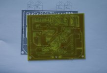
I forgot the additional decoupling capacitor and previous layout missing c4 and two diode for protection.tomorrow I will post it
regards,
joel
Hi Harrison,
I forgot the additional decoupling capacitor and previous layout missing c4 and two diode for protection.tomorrow I will post it
regards,
joel
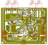
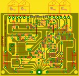
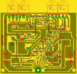
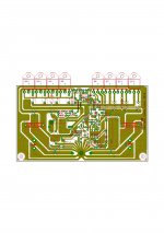
latest pcb for ksa992 and mpsa92
Hi Harrison,
Previous layout of ksa 992 pin configuration is wrong it should be ecb however mpsa92 can be used.I also forgot to include c4 and the 2 protection diode.In this latest layout I have produced two boards for ksa992 and mpsa92 and also included your suggestion.I have included also my schematic as reference.
regards,
joel
p.s.
pls. check my work.
Attachments

right.
Hi Paul,
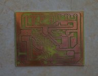
Just after removing those unwanted copper check with VOM those pads and tracks which are close to each other.This is my procedure before populating it with parts.Goodluck and enjoy DIY'ng😉.
regards,
joel
Hi Paul,
Just after removing those unwanted copper check with VOM those pads and tracks which are close to each other.This is my procedure before populating it with parts.Goodluck and enjoy DIY'ng😉.
regards,
joel

that was fast!
Hi Paulo,
Use plastic spacer on both sides of pcb and copper spacer on star gnd connected to chassis.the smaller in length much better.
regards,
joel
Hi Paulo,
Use plastic spacer on both sides of pcb and copper spacer on star gnd connected to chassis.the smaller in length much better.
regards,
joel
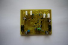
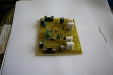
Progress
Hi guys,
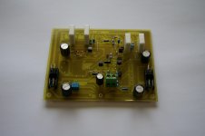
Today I soldered some parts and I'm still waiting for some resistors wich I expect to arrive tomorrow.
I noticed in the schematic R10 and R11 are switched but ok in the layout.
The diodes D1 and D22 are labeled as 1N5333. This kind of diode is a zener but the voltage is not mensioned. Wich voltage zener should I use?
kind regards,
Paulo.
Hi guys,
Today I soldered some parts and I'm still waiting for some resistors wich I expect to arrive tomorrow.
I noticed in the schematic R10 and R11 are switched but ok in the layout.
The diodes D1 and D22 are labeled as 1N5333. This kind of diode is a zener but the voltage is not mensioned. Wich voltage zener should I use?
kind regards,
Paulo.
Attachments
Thank you, astankov! 🙂
But does a 3.3V zener makes sense where it is? Shouldn't be instead non-zener protection diodes?
But does a 3.3V zener makes sense where it is? Shouldn't be instead non-zener protection diodes?
Last edited:
that is mur not zener
sori paulo I forgot to change the value.look in my past thread I have mentioned the value.Im using cellphone could not check schematic.
Thank you, astankov! 🙂
But does a 3.3V zener makes sense where it is? Shouldn't be instead non-zener protection diodes?
sori paulo I forgot to change the value.look in my past thread I have mentioned the value.Im using cellphone could not check schematic.
- Status
- Not open for further replies.
- Home
- Vendor's Bazaar
- Combined Onaudio thread. (23 threads)