I think JFET input will hot because
Vc= (33/(56+33)xVcc)-0.6 # 26V,
I2c = 2mA x 2 unit = 4mA
P2c= 112mW => Hot => have DC at output.
DC at output depends on how the feedback loop is designed. Can you show us the feedback loop used in the three models?
Yes, they have different configurations. The schematics all have revisions so if those revisions ever was used we do not now. The MPSA42/92 are rated at 625 mW so I think it is not a problem.
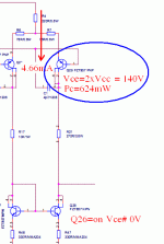
No,This case is examined in a static mode,dynamic mode is not true because when the bottom NPN on saturated,Vcc of the top PNP is # 2xVcc = 140V
Pc on the NPN : Pc= 4.46mA x 140V = 624mW # Pc max MPSA42/92.
Very easy to fire, explosion 😉
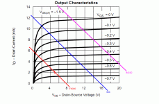
This is Rload line of 2N5565 in 3 cases T5000,M3,M330.
M330 is almost less than linear the 2 cases other.
M330 is almost less than linear the 2 cases other.
Attachments
Last edited:
I always support you, so sorry that you are not active in the VNAV forums, I don't know anything was done in your problem , but I always support you .
Try to up .
i'm a fan of you .
Try to up .
i'm a fan of you .
No,This case is examined in a static mode,dynamic mode is not true because when the bottom NPN on saturated,Vcc of the top PNP is # 2xVcc = 140V
Pc on the NPN : Pc= 4.46mA x 140V = 624mW # Pc max MPSA42/92.
Very easy to fire, explosion 😉
Can you show where in the schematic this problem can be found?
I always support you, so sorry that you are not active in the VNAV forums, I don't know anything was done in your problem , but I always support you .
Try to up .
i'm a fan of you .
Thank you interested
I have problem not fun in there,I do not want to contribute more posts there.
Well, do not dilute the topic, if you have any questions for technical of Goldmund myclone,you can ask me in here.
Regards,
Can you show where in the schematic this problem can be found?
Here
Q26=on => Vce(Q26)#0V
Vce(Q29) = 2xVcc = 140V
while the current of Q29 is 4.66mA
=> Pc (Q29) = 624mW
Attachments
How do the load line in post123 fit with the data in the recent posts?
We are discussing BJTs and yet post123 is clearly referring to FETs.
The upper limit of the posted load line graph is 20Vds. How does that relate to the 70Vce and 140Vce that you are stating?
We are discussing BJTs and yet post123 is clearly referring to FETs.
The upper limit of the posted load line graph is 20Vds. How does that relate to the 70Vce and 140Vce that you are stating?
Mr. Hien, so sorry for your problem in vnav.🙂
I'm want to ask you few questions. Why in your schematic, between post #25 and schematic in post #100 have a difference? In post #25 gate resistors of power mosfet connect different gate resistors in post #100. What's right?
I'm want to ask you few questions. Why in your schematic, between post #25 and schematic in post #100 have a difference? In post #25 gate resistors of power mosfet connect different gate resistors in post #100. What's right?
Here
Q26=on => Vce(Q26)#0V
Vce(Q29) = 2xVcc = 140V
while the current of Q29 is 4.66mA
=> Pc (Q29) = 624mW
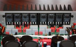
This is not a problem, the FZT957 in your schematic can handle 3000mW
(3W) total power. But only if coold off by the PCB, see picture. You can not replace this part with one MPSA92. (it will get too hot) But the MM9.2 and the chinese clone uses one MPSA92 in this position. That's why goldmund changed to FZT in later models.
Attachments
Of course no problem with FZT.This is not a problem, the FZT957 in your schematic can handle 3000mW
(3W) total power. But only if coold off by the PCB, see picture. You can not replace this part with one MPSA92. (it will get too hot) But the MM9.2 and the chinese clone uses one MPSA92 in this position. That's why goldmund changed to FZT in later models.
I also had disputed the use of MPSA for Vas on another forum,very easy to damage 😀
Last edited:
How do the load line in post123 fit with the data in the recent posts?
We are discussing BJTs and yet post123 is clearly referring to FETs.
The upper limit of the posted load line graph is 20Vds. How does that relate to the 70Vce and 140Vce that you are stating?
No,my opinion is difference selected the voltage value in the cascode stage of models Goldmund.
It explains why the Chinese clone must use heatsink for 2N5565
It is not related to all post about Vas
Many DIYer clone by circuit M330#M9.2,... I think the circuit is not good by choosing Vb cascode (supply voltage Vd to the 2N5565) is not very reasonable not linear(Vs circuit M3,T5000,...),to explain the differences at value resistance couples(R1,R15).Tommy1000 ask me in the post#108.Well, why have you posted the information shown in post123?
Last edited:
The gate resistor in post 25 and post 100 exactly the sameMr. Hien, so sorry for your problem in vnav.🙂
I'm want to ask you few questions. Why in your schematic, between post #25 and schematic in post #100 have a difference? In post #25 gate resistors of power mosfet connect different gate resistors in post #100. What's right?
In post 25 resistor 220ohm was drawing the wrong,I am confused on the circuit principle but was corrected when layout.
Some people on your forum said that they have the original circuit but i see the their circuit mistakenly same as me.😡😕
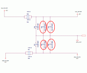
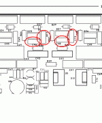
There are two small red capacitors around each driver. I can not find them in the metis schematic? Can you show me where they are?
There are bypass capacitor for Vcc(driver).It is 100nF/100V MKS2 Wima
Vcc(power) and Vcc(Driver) not direct connection together.It is connected through resistor,only Metis3 so
Here
Attachments
Last edited:
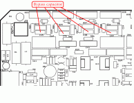
Thanks, but the schematic says C45,C46, C48 and C49? What about the others?
I am wrong,bypass capacitor is C45,C46,C48,C49
On layout
Attachments
- Status
- Not open for further replies.
- Home
- Amplifiers
- Solid State
- Clone Goldmund Amplifier