Since three 300Ohm all burned, you should double check the resistors in the front circuit, MPSA18 and MPS4250 emitter resistors R123 & R119 100 ohm each, driver MOSFET gate resistors R1 & R4 200 ohm each
Hallo Patrich et all
maybe i have a early MK 1 version of the CA 301 amplifier.
Interesting finding instead of a the 3.3V Zener mentioned in the circuit diagram,
i actually found that both zener diodes are 1N5342 6.8V.
I think i was missleaded and the 6.8V zeners were actialy not defective.
Question is what to do keep the 6.8V or replace them all with the 3.3V zeners?
All the best Ernst
if both zener diodes 1N5342 are not defective, you can keep using them
if your model using the same driver MOSFET part number then 6.8V or 3.3V zeners both ok
in normal working condition the zener diode has no function until an abnormal high voltage input it will clamp the voltage to protect the MOSFET
if your model using the same driver MOSFET part number then 6.8V or 3.3V zeners both ok
in normal working condition the zener diode has no function until an abnormal high voltage input it will clamp the voltage to protect the MOSFET
Well, I've been busy for the past 5 years. LOL I just had a chance to take another crack at this thing. I got some new lateral mosfets with some colored dots on them for matching. I built a jig for the preamp sections and I'm confident I've got bad 2SK389 and 2SJ109 on both boards! I set it up just like @patrick101 instructed in #13. I should have seen roughly 26 volts PP out for 1 volt PP in, but nothing! Oddly, DZ104 only has 1V across it after replacement and Q111 (MPSA18) and Q112(MJE340) both test good. TP4 and TP3 both had roughly 0.6V drop from the respective rails. TP5 and TP6 both have roughly 0.1V drop. I don't know how Anro1 got the measurements in #33, unless he read it wrong. TP4 and TP3 should be 0.6v from the rails. DZ104 and DZ10 are both 2.5V, I think.
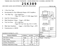
Where can I find 2SJ109 and 2SK389? I found LSK389A and LSJ689, both in TO-71 from nacsemi.com. Of course the LSJ689 is out of stock.
Also, MPSA4250 is the same? as PN4250A, which Mouser has in stock.
Where can I find 2SJ109 and 2SK389? I found LSK389A and LSJ689, both in TO-71 from nacsemi.com. Of course the LSJ689 is out of stock.
Also, MPSA4250 is the same? as PN4250A, which Mouser has in stock.


So have I, CA-2300, down on one channel, does anyone have a repair manual or schematic for this amp please?
Progress was made this weekend! I've got one channel back up thanks to @RM above. The other channel basically blew itself up and shorted out every transistor. I'm not sure why, but it might be because I started it up with a blown fuse in the MOSFET PSU during a previous attempt to fix it. Oddly, all power transistors tested OK before I started it up. The 300 Ohm resistors and power transistors are all shorted now. This thing would be easy to fix if I didn't have to deal with the MOSFET PSU.
Last edited:
I really wish this thing had better protection circuitry. If the MOSFETS didn't blow the fuses, should I be worried about damage to the preamp?
What a mess. I believe I have most transistors. 2SJ109-2SK389, MJE340-350, 10N20-10P20 and MJ21193-21194.
R
R
I've still got another set of 10P20 and 10N20. I still have one set of 2SJ109 - 2SK389. The MJ21193 and MJ21194 I can get from Mouser.
It's very important to double check the connections between the parts and both sides of the circuit board when we replacing parts in a double sided PCB.
When rebuilt the power section, insert the mosfet set 10P20 and 10N20 and only one pair MJ21193 and MJ21194 for voltage checking purpose first, after checking the voltage is ok then we can install the rest output transistors for final test and adjustment.
Note : first check all resistors and diodes in the power section if they need replacement, replace new 10P20, 10N20 and MJ21193, MJ21194 in their CORRECT positions with new thermal insulator
Good luck!
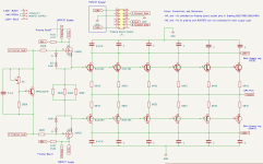
Thanks everyone for keeping up with my thread. You all have been so helpful! So, here's my latest revision. It includes corrected errors and commentary associated with the OEM schematics. I've concluded that powering the amp up without the MOSFET supply was the issue with my first repair attempt. As my schematic shows, errors with +V1 and -V1 are catastrophic.
I've designed a test setup that allows me to power the preamp via the MOSFET supply. The MOSFET section testsOK, so I added 1R3000 diodes in place of the MJ21194 and MJ21193 transistors and connected them directly to 0R33 resistors and ultimately the output. It worked just fine with test waves.
After the repair failure, the 10N20 and 10P20 tested OK out of circuit and they tested OK in my test setup up to about 55V with 25mV through the diode on each 0R33. After 55V, the current draw went pretty high. Also, I've got some spare MJ21193 and MJ21194 transistors left over from the first repair attempt that test OK. Should I put one MJ21193 and one MJ21194 back in and take it up to full power in the original power supply?
Does anyone have suggestions?
Attachments
Also, the pad for the Gate on the 10P20 pulled up and I might not have soldered it correctly on my second repair attempt. The only other thing I can think of is the bridge rectifier for the main supply on the faulty channel. Is there an easy way to test in Circuit? I'm thinking about adding a power resistor across the terminals and monitoring with a scope and some multimeters. Taking the bridge rectifier out of circuit and testing the relays is a big pain with this design.
Whatever transistor was driving the 200 ohm vaporized resistors is likely dead and maybe the bias parts as well. That explosion would've forced alot of power through the circuit.
I replaced everything associated with the 200 ohm gate resistors getting vaporized in the first repair attempt. My current problem is that the output transistors have failed instantly twice. The MOSFET circuit and MOSFETs have survived both failures. I thought the 300 ohm resistors failed, but it turns out the output transistors were shorted. The preamps survived the second repair attempt.Whatever transistor was driving the 200 ohm vaporized resistors is likely dead and maybe the bias parts as well. That explosion would've forced alot of power through the circuit.
- Home
- Amplifiers
- Solid State
- Classe CA-401 Rebuild