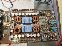
Hello, I have three amps, based on this design. What are the common drive board problems? Output fets are irf9640 and irf640n. I have high and low side drive, fets get hot quickly. On another amp, there is jo drive. Checked all parts, changed lm393, drive OK. Fets get hot. What is the right part number for the drive transistors AG and dk?
Attachments
Transistor marked DK - 2sc4672
Transistor marked AG - 2sa1797
The drive looks low. Do you have 12v across the collectors of the driver transistors?
The 470 ohm resistors, the small drivers and the larger driver transistors can fail. I've seen a lot of bad solder connections on the larger transistors on these boards.
Transistor marked AG - 2sa1797
The drive looks low. Do you have 12v across the collectors of the driver transistors?
The 470 ohm resistors, the small drivers and the larger driver transistors can fail. I've seen a lot of bad solder connections on the larger transistors on these boards.
Last edited:
Thanks for the info. Yes I have 12v between collector. But sometimes oscillation disappear and the amp goes into protect.
If I measure between gate and source, it shows 8 to 12 v. Then after a second or longer, oscillation starts, and the voltage drops to 4v.
If I measure between gate and source, it shows 8 to 12 v. Then after a second or longer, oscillation starts, and the voltage drops to 4v.
The fets are out of circuit. I have one 470 ohm resistor beside 1d q22 transistor, which shows 440 ohm. The resistor is OK..
Do you have something in your tutorial about that?
Do you have something in your tutorial about that?
Last edited:
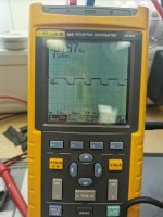
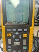
Part of the confusion may be that the feedback loop is open. Normally you would jump terminals 1-2 of the TL072 but yours is covered. That would give you approximately equal drive (pulse width). The first waveform that you have posted seems low in amplitude but also has a wider pulse width than I'd expect, looking at the second waveform.
Connect a load across the speaker terminals and see if the waveforms have equal width after the relay closes.
I'd replace the resistor.
When you get the amp working, confirm that every FET has the same drive in each bank. There are 4 drive circuits and the amp will seem to be working correctly even if 3 groups in that bank have no drive.
I have a 10ohm resistor in the terminal. One bank of fets is mounted, the other bank not. First group of where the irf9640 are normally mounted shows lower voltage then the other groups of irf9640 and irf640n. Anyway it seems to low voltage at all.
I changed the 470 ohm resistor, now it shows 450 ohm. All other shows exactly 470 ohm..
I changed the 470 ohm resistor, now it shows 450 ohm. All other shows exactly 470 ohm..
Attachments

So, i checked again. It's only 3v between gate and source. But the working side has the same voltage.. Only one group of fets in a bank is lower. I expect, that this also is a problem from the value of the 470 ohm resistor.. I have to check, why the value is dropping.
Maybe you have a leaky transistor that's causing the resistor to read out of tolerance.
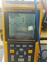
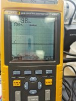
Where is ground on your scope? For the first image you posted, the scope was set right but now you've changed it. Without knowing where ground it, the waveforms are absolutely useless.
Set the vertical amplifier back to 5v, or even 2v if the waveforms will fit on the display with the trace aligned to the reference line (at the vertical center of the scope).
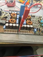
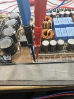
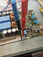
Assuming that the scope has no connection to the mains, place the black/ground probe on the source leg of the FET that you're getting the waveform from.
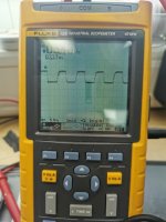
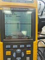
Where is ground on your scope? For the first image you posted, the scope was set right but now you've changed it. Without knowing where ground it, the waveforms are absolutely useless.
Set the vertical amplifier back to 5v, or even 2v if the waveforms will fit on the display with the trace aligned to the reference line (at the vertical center of the scope).
Assuming that the scope has no connection to the mains, place the black/ground probe on the source leg of the FET that you're getting the waveform from.
Hello Perry, the scope ground was at the source. I removed the drive board from the Mainboard, now the resistance is OK.. I think I have to check on the Mainboard.
Found a leaky transistor on the drive board. Now the value are OK.
Attachments


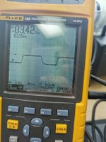
Without knowing where ground is on the display, the waveforms are useless. I don't know every scope. I'm assuming that you didn't center the trace and the black line is the ground. If so, the drive is likely OK. Remember to check the drive to every FET when they're installed.
The top-bottom of the waveforms should be there. If the scope trace is actually referenced to the center vertical line, the waveforms look like there is a significant DC offset which would cause excessive current draw. I think the scope settings are wrong and the short black line is the ground.
I will recheck the scope settings tomorrow. But i think you are right with the dc offset, because with only one bank mounted i have allready a current draw from 2,6 Amps..
The DC Offset can come only from leaky transistors i think, but they are all measured ok, also the diodes on the drive board. Maybe the LM 393 is damaged?
The DC Offset can come only from leaky transistors i think, but they are all measured ok, also the diodes on the drive board. Maybe the LM 393 is damaged?
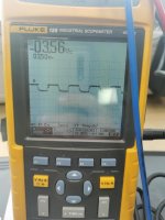
You are sure, that all waveforms top should be at the Center Line (A)? The Amp has P-Channel and N-Channel Mosfets.. I think its correct. I only dont understood, why the osciloscope shows only 3,6V, when i have 1 3/4 fields ore dividers, which should be 5V/div.
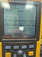
Half are driven from the positive rail (source leg) down 10v. With the black probe on the source, the waveform should go from the reference line down.
The other half will be driven from the negative rail up 10v. That waveform should be from the reference up 10v.
The voltages above are amplitude as seen on the display, not the readout.
What does your scope show on the emitters (tied together so you only need one) of Q14 and Q18 and the two collectors of those transistors? Black probe on the secondary ground.
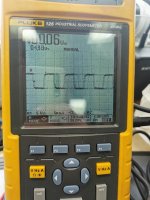
Those look OK.
The amplitude of the drive signal comes from the next stage (the row of small transistors connected to the 470 ohm resistors). The ratio of the 1k to the 470 gives the amplitude. The amplitude is generally about 2:1.
Confirm that R24 is within tolerance.
The amplitude of the drive signal comes from the next stage (the row of small transistors connected to the 470 ohm resistors). The ratio of the 1k to the 470 gives the amplitude. The amplitude is generally about 2:1.
Confirm that R24 is within tolerance.
- Home
- General Interest
- Car Audio
- Class d amps, based on this design troubleshooting