It helps a lot to first consider classes A, B and C as defined for a single transistor.
Class A : full conduction during both alternances.
Classe C : conduction during less than one alternace.
Class B : conduction between one alternance, no more, no less. It is a theorical case because it is impossible to reach and maintain.
In push-pull mode :
- a Class AB has full conduction on both alternances at low levels. At high levels, only one branch is conducting at a time. So the output impedance of the push-pull is not constant during a full cycle. The problem is known as gm (transconductance) doubling.
- theorically, as seen above, pure Class B is not possible. But an optimal bias can give a quite constant output impedance, and then has the lowest distortion at high levels. It is this that most people now agree to call class B. To avoid confusion, it may be called "optimally biased class B".
Self:Class-B (optimal bias) = Cordell:Class-AB (optimal bias)
Self:Class-AB = Each device will conduct between 50% and 100% of the time, avoid to use
Cordell:Class-B = Under-biased amp (less than optimal bias)
LKA:Class-B = few mA bias (1-5mA)
Self:Class-AB = Each device will conduct between 50% and 100% of the time, avoid to use
Cordell:Class-B = Under-biased amp (less than optimal bias)
LKA:Class-B = few mA bias (1-5mA)
Last edited:
for my two penn'orth a Class B amplifier with a small bias to minimise crossover distortion, you might say optimally biased, is Class AB as it will operate in class A at very low output levels. It effectively works in Class B at higher output levels.
you might say a Class B amplifier is one where the bias is absolutely minimum but not optimally so, such that it works in almost Class B mode down to low powers. An underbiased Class B amplifier really isn't Class B because each output device is conducting for less than a half-cycle and is really more Class C, but with two half-cycles.
you might say a Class B amplifier is one where the bias is absolutely minimum but not optimally so, such that it works in almost Class B mode down to low powers. An underbiased Class B amplifier really isn't Class B because each output device is conducting for less than a half-cycle and is really more Class C, but with two half-cycles.
It seems there are 2 suggestions; one suggested class AB, two suggested class B.
Also, seems it has 2 suggestions about class identification; one classified by bias, two classified by angle.
IMHO, shall we move to use the angle to solve the conflict? And, could anybody provide illustrations or explanations along with this matter, please?
Also, seems it has 2 suggestions about class identification; one classified by bias, two classified by angle.
IMHO, shall we move to use the angle to solve the conflict? And, could anybody provide illustrations or explanations along with this matter, please?
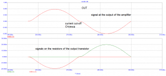
Yes, it seems that I showed you earlier the cut-off of the collector current of the Class B mode. Just on a very similar output stage on a parallel amplifier with a powerful diamond buffer.With a shunt and a regular one .I can show you if there is any doubt .It seems there are 2 suggestions; one suggested class AB, two suggested class B.
Also, seems it has 2 suggestions about class identification; one classified by bias, two classified by angle.
IMHO, shall we move to use the angle to solve the conflict? And, could anybody provide illustrations or explanations along with this matter, please?
Last edited:
No conflict if you include "optimally biased class B" in the terminology. We must not be too obsessed by classes.IMHO, shall we move to use the angle to solve the conflict?
Output impedance vs amplitude is the main thing to look at : ideally it should a straight line. The real aim of Quad 405 current dumping (class A + class C) is to get this straight line using a feedback mechanism including a bridge.
Obviously this is a semantic argument. Operation classes are defined formally in electrical engineering, particularly in the RF power field, but the definition is based on a single-ended power device, probably transformer coupled to an antenna load.
Class A means the device is always conducting current to the load, i.e, 100% of the time.
Class B means the device is conducting exactly 50% of the time. (This has probably always implied some sort of push-pull arrangement.)
Class C means the device is conducting less than 50% of the time.
These definitions have been adapted to complementary power stages wrt each half of the output, p-channel or PNP, and n-channel or NPN. If you have some bias current in the output drivers, then they each conduct slightly over 50% of the time, so it's technically not class B. At some low level of signal, the output stage will operate class A. Above that, is it class B? No, the definition of class B is 50% conduction. So, many decades ago, engineers decided this class-B plus bias should be called class AB, because it's somewhere between the two.
No device has 50% conduction in practice.No, the definition of class B is 50% conduction. So, many decades ago, engineers decided this class-B plus bias should be called class AB, because it's somewhere between the two.
As far as I know, usual op-amps have always been said working in class B and have a small quiescent current.
Class AB is identified by GM doubling which is not often found on commercial amplifiers.
The terminology has been revised by Douglas Self and is now unambiguous.
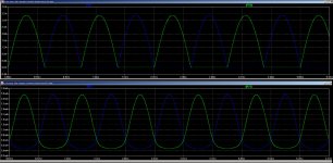
If the two simulations are seen at first glance, one could say: Clearly, the first plot is class-B and the second is class-AB. Ultimately, it's the same amplifier at different levels ...
I don't think the classification is that important. Tell me how much quiescent current a complete amplifier causes, that's enough for me.
If a class G / H circuit is included, then I know that the amplifier works even more efficiently. I don't need any more information, I can measure the rest.
I leave the question of which class it is ultimately to the nit-picker 🙂
Attachments
If the two simulations are seen at first glance, one could say: Clearly, the first plot is class-B and the second is class-AB. Ultimately, it's the same amplifier at different levels ...
I don't think the classification is that important. Tell me how much quiescent current a complete amplifier causes, that's enough for me.
If a class G / H circuit is included, then I know that the amplifier works even more efficiently. I don't need any more information, I can measure the rest.
I leave the question of which class it is ultimately to the nit-picker 🙂
On my more graphs, the VC works in class B mode with closed output transistors . However, this is only noticeable when modeling a single VC that is not covered by the OOS. a large loop gain eliminates the effect of too little quiescent current.Change in quiescent current from 0.2 ma to 5mA


Attachments
Last edited:
Larger open loop gain cannot possibly compensate for insufficient idle current. There is zero gain in the dead crossover region unless you close it with just enough idle current.
And if we provide conditions for this ? It can.Larger open loop gain cannot possibly compensate for insufficient idle current. There is zero gain in the dead crossover region unless you close it with just enough idle current.
Define 'provide conditions for this'. Conditions such as what? If there is no gain there is no NFB. No way of correcting the error.
Simplex exemplum.Output transistors clausa sunt.Sed nulla est intervalli . Ego delete post imaginem


My Latin is OK but my Russian not. This forum is conducted in English thanks. I don't understand your graphs or your point. If you have no open crossover region you have adequate idle current, by definition.
Sorry,glitch in the translator . A graphic example.The output transistors are closed .There is no collector current cutoff . I'll delete the images later.
The quiescent current A1943/C5200 is 2mA.The picture does not change even at a rest current of 0.5 ma. Without the capacitor, the cut-off.
hint: If you look at the VAS voltage instead of the power output you find the inverse of the cross-over distortion, magnified by the neg feedback. Here you can observe the effect of biasing through a magnifying glass.😉
VAS signal / more clearlyhint: If you look at the VAS voltage instead of the power output you find the inverse of the cross-over distortion, magnified by the neg feedback. Here you can observe the effect of biasing through a magnifying glass.😉


Last edited:
- Home
- Amplifiers
- Solid State
- Class B Amplifier