Depends on how accurately you want to calculate the die temperature. Starting with the chip, the emitter-base junction is at the top, so there is the silicon chip thermal resistance to consider first. The power will be largely dissipated in the collector-base depletion region, but unless you dismantle a transistor to measure its physical properties you don't know how thick the chip is. Probably not too thick (100microns?) as that is one way manufacturers have got thermal resistances down. Then the interface to the package header, the package header resistance to mounting base; the thermal resistance of any interface to and of the insulation used. then the heatsink. Each of these has a thermal mass as well, so the equivalent circuit is one of several time constants represented by an R (thermal resistance) and C (thermal capacity) for each. Some of these time constants are small (thermal mass of silicon and thermal resistance) while others (heatsink) are large.
It may be possible to determine some of the main time constants from published thermal impedance data - the graphs showing transient thermal impedance as a function of pulse width.
But then as you indicate, there is the consideration of the demand placed on the device. A reactive load will cause the transistor to disspate more than it may want, with having to pass high current at high voltage, so it depends not just on the signal levels and duty cycle but the actual load impedance.
Yes this can be done but it is more often the case that we just use average thermal impedance data as published and make a best estimate for the transistor power based on expected loading.
I can't fully remember info from my extensive reading of wireless world when it was in circulation but in class B power dissipation was calculated on the basis of the RMS power measured at 1khz multiplied by a factor I can't remember. Continuous power, not music or din. It's an area that caused me some confusion - how to do it. When the factor was mentioned several designs agreed. It's like a lot of similar areas a metric. Max distortion is another just measured at 1khz which also relates to the rms power. 🙁 Or one of the others.
In class AB at full RMS power all of the class A power must be going into the speakers as the output currents are higher than it can give but when a sine wave is being produced some proportion of the wave will be produced with class A. That dissipation of that proportion will be highest at a level of zero on the wave.
Posting has dug up where the class B factor comes from. It's simply the DC equivalent of the sine wave. That will still apply when a class AB is running in pure B. But each time a sine wave passes into the A region that will increase dissipation, highest when it is at zero.
🙂 My head hurts now. If the A and B regions are split the wave forms causing dissipation are no longer a pure sine, One way might be to assume the class A is more or less a square wave and add that to rms dissipation calculated in pure class B. That will be simply 1/2 it's peak to peak if it was pure square wave. I suppose part sine waves can be integrated - pass.
Thinking a bit further it wont be a pure 50 50 square wave it will be some other ratio based on the time out of class B while in class A. It should be possible to do something with that. More like a repetitive square pulse with a high off time.
I believe in Class A, no output completely cuts off--- each output device conducts at least some current, is always biased into the conducting state, is always "active." In contrast, the devices in class AB both conduct within the crossover region but then one output enters cutoff while its opposite delivers the load current when the signal drives the amp into class B conduction.
A low amplitude square wave could lie completely within the class A region in the crossover region; higher amplitude would drive into class B except in very brief transitions though crossover.
Thinking a bit further it wont be a pure 50 50 square wave it will be some other ratio based on the time out of class B while in class A. It should be possible to do something with that. More like a repetitive square pulse with a high off time.
A low amplitude square wave could lie completely within the class A region in the crossover region; higher amplitude would drive into class B except in very brief transitions though crossover.
Last edited:
The way I see it look at the shape of a sine wave, In class B the standing current is small so not worth considering.
When in class A part of the sine wave period is powered by transistors that are " fully on" so the difference in power dissipation over class B is a sort of inverted triangle standing on it's tip. Hypotenuse formed my the sine - more or less a straight line. Area and class A current -> the additional power.
The question then is what happens if the total drive is reduced and the power dissipation in class A is high enough to exceed the max drive number obtained as above when the 2 are summed. Gut feeling is that it wont what ever level class a is set at.
😉 I do remember being annoyed with myself when some one mentioned how class B was calculated. Effectively rectifying the sine and working out it's true rms value. Pretty basic stuff really.
Frequency. It could be done at any so assume the old favourite was used. 1 khz. I may have read that or I may not have,
I suspect I would sketch it out and eyeball and equivalent pulse to the triangles, Some simple sine maths assuming a straight line may be possible. Probably is.
However its a theory that makes sense to me but mine and like all I can make mistakes. Maybe it could be checked via class A efficiency. The rms of the sine can can be calculated but the current is DC at supply voltage. With class B I suppose the power going in has to be measured compared with what comes out to the speaker. Same with D.
I.m confused by your explanation of your confusion.
Class A has transistor(s) always conducting, so the output is due to an increase or decrease in current with a corresponding change in voltage. Class AB can be considered as ideal Class B as you suggest where the current flows into the load and the voltage across the transistor passing the current reduces.
The power supply, in either case, delivers a sinewave current at a constant voltage, so it isn't the RMS you need for the input power but the average current.
I believe it's a misconception to assume that class A amps have to be inefficient, prodigious heat generators. To be considered class A, the driving transistors simply have to be conducting current continuously. I believe efficiency is often governed by the driving circuitry. I offer two examples having reasonable efficiency.
The first is Figure 19 within the LF1166 data sheet, linked below. It delivers 100W into 8 Ohms with +/- 50V supplies. The data sheet doesn't taut it as being class A, but it is--- its whole concept is to control device outputs so that neither output device ever enters cutoff. The data doesn't specify quiescent bias current, but I believe it's 20mV/0.22 Ohm, i.e. about 91mA or about 9.1W from the dual supplies. Modest, I contend.
https://www.analog.com/media/en/technical-documentation/data-sheets/1166fa.pdf
The second example is the Sumo Nine, attached below. It's explicitly claimed as a class A design, delivers 70W into 8 Ohms. It uses a bridge drive topology with each driving arm being having class A drive. It's quiescent bias current isn't specified, but I believe it's about 20V/(5K pot//5.1K + 1.6K). That is at most about 12.5mA. That's comparable to class AB efficiency.
Attachments
Last edited:
In practice it will have some degree of ripple.so it isn't the RMS
"Now consider a following example. I have a heatsink with which a constant power dissipation is made of 50W with mosfets on it. Then the heatsink temperature raises 15 degree above room temperature of consider 35 degree C to heatsink temp 50 deg."I`m wondering looking at a FEA simulation the heatsinking size of a Pure class A is accurately estimated by giving constant power dissipation and right thermal conductivity constants and we do get perfectly right with tolerance of +/-0.5 deg C when data is given properly.
This means you have a heathsink with 15°C/50W=0,3°C/W (or K/W).
"Now consider the same heatsink how much it can dissipate when it comes to class AB where the idle current temp of heatsink rose by just 3deg C in AB mode. Now what I would like to know is that how much Class AB heat does the heatsink takes up for same AB."
At idle the AB amp is dissipating 3°C/0,3°C/W=10W. So, depending on the output-stage topology (switching class AB, various non-switching) you still have about 40W left to dissipate with signal for the same temperature rise.
This is only a rough estimation assuming thermal resistance of the heathsink not varying with temperature.
Last edited:
Now are you talking about actual efficiencies or theoretical?In practice it will have some degree of ripple.
At one point you seemed to be talking about theoretical but it wasn't clear if you really meant ripple voltages.
If you are talking about a power supply, unregulated, which has a voltage variation (even a regulated supply will have ripple) then the power has to be integrated with the ripple voltage and current. In the main if the ripple voltage is small, as you would expect a decent PSU to provide, then it still amounts to the average current input for the applied power.
Some points: if the amplifier draws a constant current then the power supplied by a PSU with a ripple voltage is still dependent on the average voltage.
If an amplifier draws current dependent on the PSU voltage (which should not apply to the main signal power but smaller pre-stages might, but would be expected to be filtered) then a small variation of voltage only has a second order dependence on ripple voltage so is still, mainly the average. The operative word being "small" in that the ripple should not be large compared with the PSU nominal voltage.
By "constant current" this does not mean a Class A specifically, but a signal which is not dependent on the power supply voltage. You can think of a Class AB amplifier or idealised Class B providing a low frequency sinewave where the peak extends for several cycles of mains, or the average of a much higher frequency.
Alright now here we are cornering well."Now consider a following example. I have a heatsink with which a constant power dissipation is made of 50W with mosfets on it. Then the heatsink temperature raises 15 degree above room temperature of consider 35 degree C to heatsink temp 50 deg."
This means you have a heathsink with 15°C/50W=0,3°C/W (or K/W).
"Now consider the same heatsink how much it can dissipate when it comes to class AB where the idle current temp of heatsink rose by just 3deg C in AB mode. Now what I would like to know is that how much Class AB heat does the heatsink takes up for same AB."
At idle the AB amp is dissipating 3°C/0,3°C/W=10W. So, depending on the output-stage topology (switching class AB, various non-switching) you still have about 40W left to dissipate with signal for the same temperature rise.
This is only a rough estimation assuming thermal resistance of the heathsink not varying with temperature.
As per that requirement of 33.96 W of dissipation and if the heatsink with 15°C/50W=0,3°C/W (or K/W) and heatsink capability is about 40W then this should be a good heatsink for the above requirement?
Now consider we have 3 pairs of 2sc5200 and 2sa1943 in the output stage.
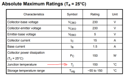
The max junction temp of the die is about 150 deg C.
Now the dissipation of the each transistor consider for 200W into 8 ohm so how does math goes in here to have safer operation.
Now as per the above case the heatsink temp raise to 50deg C. So now in the same above case how do we know what is the junction temp?
Attachments
To recap: you have to decide what parameters you want to base your heatsink on. Is it going to be "music power", with (perhaps) 10:1 peak to mean power ratio; is it going to allow for a reactive load and if so what value; is it going to be rated for maximum (inefficiency) of a Class AB amplifier (which has peak dissipation at around 40% rms output); a worst case signal (square wave half supply voltage output) or something else?
Is this an amplifier you would want for yourself or to make/sell?
If sell, it had better be able to withstand (say) 40% full power for at least an hour without overheating. If for yourself, then are you always going to be able to keep the volume low enough or music power to the design limits you may have set?
Will you have overtemperature cut-outs for a small heatsink? Or a peak detector for example?
As many have posted earlier, it really is up to you to make the decision. Then build and evaluate to see whether your decisions were right.
Another point to bear in mind is that really there is no "overspec'd" heatsink. Transistors will fail after some thousands of thermal cycles and the cooler you run them the longer they will last. If you do have a large heatsink your amplifier should last longer. Many high reliability computer systems were said to limit the junction temperatures of the chips to 55C. I don't know if that rule is generally applied these days. That would need a large heatsink for an amplifier of significant power.
To answer your question which overlapped with my post the junction temperature is dependent on the thermal resistance of the transistor and any insulator you use to insulate it. For the C5200 it's 0.83K/W and your insulator might be 0.4K/W (some new silicone insulators might be as low as 0.2K/W).
If your 8 ohms is a pure resistive load and the power 200W (rms I assume) then taking the worst case output (say 40%) the dissipation with sinewaves is going to be around 80W. This power is dissipated between all of your output transistors i.e. 13.33W each. That means the junction temperature would be 13.33x1.23 or approx 16.5C above the heatsink. Your heatsink has to dissipate full whack 80W. If you let Tj=150C that means the heatsink must be 150-16.5=133.5C (hot enough to cook your egg, not, I think, to be recommended) so needs to be (if we say 30C room temperature (outside on a hot sunny day perhaps) the total temperature change is 133.5-30=103.5C. The thermal resistance should therefore be 103.5/80 or 1.3K/W.
However, that does not allow for any margin or different operating conditions. You may - or even should - consider a heatsink temperature much lower. Your 50C would be OK but means having a thermal resistance of 50/80=0.625K/W. This calculation excludes the quiescent current dissipation which can be added on. It excludes reactive loads, lower loads, etc etc as mentioned in my earlier post. The actual temperature still needs room temperature added.
With 200W output what is more of a concern is the second breakdown rating of the transistors. Once above the breakpoint you may need more devices in parallel. That is, in particular, a point to consider when contemplating a reactive load.
What is never mentioned with a reactive load (as far as I have seen; Self or Cordell may have) is the frequency of your assumed reactive load. Since reactive loads apply at some frequency, you can moderate the SOA with a considered repetition rate which helps. I've not seen that commented on.
(The 40% is not the theoretical peak dissipation of a Class AB - that's nearer 30%, but with quiescent current it could easily be as high as 50%).
Sorry to burst your bubble, but that's not Class A operation. Once the output current exceeds twice the quiescent current one output device will be completely off and the other will conduct all the current. That's Class AB. That's no different than any other Class AB amp.The first is Figure 19 within the LF1166 data sheet, linked below. It delivers 100W into 8 Ohms with +/- 50V supplies. The data sheet doesn't taut it as being class A, but it is--- its whole concept is to control device outputs so that neither output device ever enters cutoff. The data doesn't specify quiescent bias current, but I believe it's 20mV/0.22 Ohm, i.e. about 91mA or about 9.1W from the dual supplies. Modest, I contend.
There're lots of misconceptions around Class A vs AB vs B. I tend to follow Douglas Self's definitions. You can find them in the Output Stage chapter of his power amps book.
In Class A all output devices conduct some current at all times. When the load current is zero the maximum current flows in the output stage. That's why Class A amps are such heat generators. Basically a Class A output stage dissipates P = 2*VCC*Iload(max), minimum, assuming a symmetric bipolar supply where VEE = -VCC. The advantage of Class A is that it cannot have crossover distortion. But also note that crossover distortion is not the only distortion mechanism out there.
In Class B at least one output device conducts at any given time. If you were to hold the output of a Class B amp at exactly zero volt (and everything was balanced) both output devices would just barely be conducting. Such a "zero bias" Class B output stage would also not have any crossover distortion as the two output devices take turns conducting the current with zero overlap between them (and also zero dead zone).
Unfortunately such a "zero bias" Class B output stage also only exists in theory. Even if you could adjust the bias such that the outputs just start to conduct at idle the bias could quickly drift off of that ideal point once the temperature changed. So we dial up the bias a bit (and make it track the temperature of the output devices).
A properly biased Class B output stage also does not suffer from crossover distortion. But it does suffer from distortion due to gm-doubling in the output stage whereas the Class A output does not. In the properly biased Class B output stage one output device conducts during the positive half of the signal swing and the other conducts during the negative swing. Both devices conduct during for a good chunk of the region around the zero crossing. The switch from one device to two and back to one changes the gain of the output stage slightly. This slight change is enough to cause some low level of distortion. That's not the same as crossover distortion, however, as both output devices in a Class B output stage conduct at the zero crossing, just as they do in Class A.
It turns out there is an optimal bias point for a Class B output stage. You can see Doug Self's book for the derivation. Basically you need to tune the bias for VT = kT/q across each emitter resistor in a bipolar output for the lowest distortion. Done! There might be a similar optimum for a MOS output, but Doug's not a MOS guy so you'll have to read Cordell for that. 🙂
Marketeers have figured out that "Class A" sells, so how about cranking the bias current in a Class B output up a bit? Douglas Self calls this Class AB. Sure. That does create a larger region of Class A operation, but the distortion caused by the gm doubling is made worse, so the overall performance of the output stage is worse that it would be had it been biased for Class B operation.
I think the confusion around amplifier classes arise because some insist that a Class B output stage must have a dead zone, hence, must create crossover distortion. But, technically, that's Class C. In Class C none of the output devices conduct for some part of the signal swing.
Tom
I'm an admirer of your work but, in this case, I must respectfully disagree. Below is text from the LT1166 data sheet explaining the principle of the bias control.
Best,
Steve
Multiplier Operation
Figure 2 shows the current multiplier circuit internal to the LT1166 and how it works in conjunction with power output transistors. The supply voltages VT (top) and VB (bottom) of the LT1166 are set by the required “on” volt- age of the power devices. A reference current IREF sets a constant VBE7 and VBE8. This voltage is across emitter base of Q9 and Q10 which are 1/10 the emitter area of Q7 and Q8. The expression for this current multiplier is:
VBE7 + VBE8 = VBE9 + VBE10 or in terms of current:
(IC9)(IC10) = (IREF)2/100 = Constant
The product of I and I is constant. These currents are C9 C10
mirrored and set the voltage on the (+) inputs of a pair of internal op amps. The feedback of the op amps force the same voltage on the (–) inputs and these voltages then appear on the sense resistors in series with the power devices. The product of the two currents in the power devices is constant, as one increases the other decreases. The excellent logging nature of Q9 and Q10 allows this relation to hold over many decades in current.
The total current in Q7 and Q8 is actually the sum of IREF and a small error current from the shunt regulator. During high output current conditions the error current from the regulator decreases. Current conducted by the regulator also decreases allowing VT or VB to increase by an amount needed to drive the power devices.
I do agree that the bias circuit will try to enforce a constant current through the source resistors in the output stage. However, I doubt this current is set for the current required for Class A operation at 100 W into 8 Ω. If it was the IC would not be usable for Class AB (or B) operation.
Tom
Tom
The point I was attempting to make (not well) is that there doesn't have to be a large standing current at idle to have continuous class A conduction--- or the attendant inefficiency. Each driving device only has to have non-zero current to meet the definition of class A.
The Sumo Nine accomplishes analogous low standing bias by driving each half of a full power sine wave with separate class A transistors; it's opposite brother passes low standby current during its "resting" half-cycle to maintain class A. Each transistor remains active so that it can begin to supply current without having to emerge from a cutoff state.
The Sumo Nine accomplishes analogous low standing bias by driving each half of a full power sine wave with separate class A transistors; it's opposite brother passes low standby current during its "resting" half-cycle to maintain class A. Each transistor remains active so that it can begin to supply current without having to emerge from a cutoff state.
I'm with Tom on this. In an amplifier where the output stages are held on through some means of biasing during the period they would normally be off, at a low current perhaps equal to the quiescent current, then this really is a Class AB. Class A is generally taken to mean one where two devices are always on at a quiescent current Iq and the current in each device, in response to a signal, varies theoretically between zero and 2Iq. That's where (almost?) every textbook says a Class A amplifier is theoretically 50% efficient.
Peter Blomley published a design in Wireless World, Feb. 1971 where he kept the output stage ticking over instead of switching off. He called that design a Class B, but I think Tom would agree that it is really an AB. In fact it seems to me to be more representative of an AB rather than most amplifiers classified as AB where one or other of the output stages turns fully off. The definition works though because at very low level signals those amplifiers are working in class A.
Peter Blomley published a design in Wireless World, Feb. 1971 where he kept the output stage ticking over instead of switching off. He called that design a Class B, but I think Tom would agree that it is really an AB. In fact it seems to me to be more representative of an AB rather than most amplifiers classified as AB where one or other of the output stages turns fully off. The definition works though because at very low level signals those amplifiers are working in class A.
That's where I land as well. Even if the LT1166 has both output devices conducting some current, the bottom device will only conduct the idle current while the top device delivers the load current and vice versa. This means that for just below half of the signal swing one of the devices will only conduct the idle current and no signal current. That makes it Class AB (or B) in my book.In an amplifier where the output stages are held on through some means of biasing during the period they would normally be off, at a low current perhaps equal to the quiescent current, then this really is a Class AB. Class A is generally taken to mean one where two devices are always on at a quiescent current Iq and the current in each device, in response to a signal, varies theoretically between zero and 2Iq. That's where (almost?) every textbook says a Class A amplifier is theoretically 50% efficient.
Tom
- Home
- Amplifiers
- Solid State
- Class AB Amplifier heatsinking size referenced to a pure class A amplifier